background image

17

NC20 - Manual - 01 - 2015

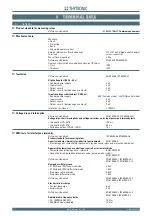
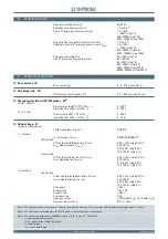
TECHNICAL DATA

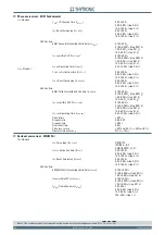
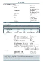
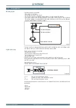
 Undercurrent - 37

[1]

I< Element

I<

def


Operating 

logic 

     OR

[2]

 Defi nite time

37 First threshold defi nite time (

I<

def

   0.05...1.00 

I

n

I<

def


Operating time (

t

I

<

def

    0.04...200.0 

s


0.04...9.99 s (step 0.01 s)


10.0...99.9 s (step 0.1 s)


100...200 s (step 1 s)

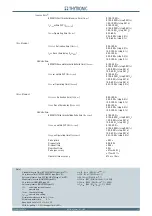
I<< Element

I<<

def


Operating 

logic 

     AND

[3]

 Defi nite time

37 Second threshold defi nite time (

I<<

def

  0.05...1.00 

U

n

U<<

def


Operating time (

t

I

<<

def

    0.04...200.0 

s


0.04...9.99 s (step 0.01 s)


10.0...99.9 s (step 0.1 s)


100...200 s (step 1 s)

Pickup time 


≤ 

0.04 s

Dropout 

ratio 

      1.03...1.05

Dropout time   


≤ 

0.05 s

Overshoot 

time 

      0.04 

s

Pickup 

accuracy      ±


0.5% with 0.1

I

n

,


±


0.2% with 1

I

n

Operate 

time 

accuracy 

     5% 

or 

±


10 ms

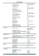
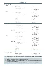
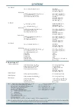
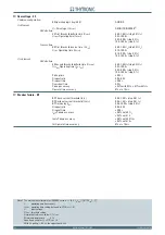
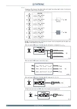
Phase unbalance - 46

I

2

>

 Element

I

2CLP

> Activation time (

t

2CLP

>) 

    0.00...100.0 

s


0.00...9.99 s (step 0.01 s)


10.0...100.0 s (step 0.1 s)

I

2

Reset time delay (

t

2

>

RES

)


0.00...100.0 s


0.00...9.99 s (step 0.01 s)


10.0...100.0 s (step 0.1 s)

Defi nite time

46 First threshold defi nite time (

I

2

>

def

)   


1...150 % (step 1 %)

I

2

>

def

 within CLP (

I

2CLP

>

def


1...150 %(step 1 %)

I

2

>

def 

Operating time (

t

2

>

def

    0.05...60.0 

s


0.05...9.99 s (step 0.01 s)


10.0...60.0 s (step 0.1 s)

I

2

>>

 Element

I

2CLP

>> Activation time (

t

2CLP

>>)    0.00...100.0 

s


0.00...9.99 s (step 0.01 s)


10.0...100.0 s (step 0.1 s)

I

2

>> 

Reset time delay (

t

2

>>

RES

)


0.00...100.0 s


0.00...9.99 s (step 0.01 s)


10.0...100.0 s (step 0.1 s)

Defi nite time

46 Second threshold defi nite time (

I

2

>>

def


1...150 % (step 1 %)

I

2

>>

def

 within CLP (

I

2CLP

>>

def

)   


1...150 % (step 1 %)

I

2

>>

def 

Operating time (

t

2

>>

def

)  


0.05...60.0 s


0.05...9.99 s (step 0.01 s)


10.0...60.0 s (step 0.1 s)

Pickup time 


≤ 

0.04 s

Dropout 

ratio 

      0.95...0.98

Dropout time   


≤ 

0.05 s

Overshoot 

time 

      0.04 

s

Pickup accuracy 


± 1% with 

I

2

 ≥ 0.5 In

Operate time accuracy  


5% or ± 10 ms

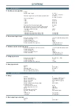
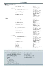
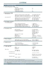
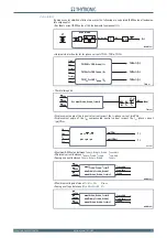
Neutral unbalance current - 46N

[4]

Common confi guration:

[5]

Compensation current (

I

C

    0.01...0.50 

I

Nn 

(step 0.01 

I

Nn

)

Compensation angle (

φ

C

)     0...359°


(step 1°)

Automatic compensation enable (ACE)   


ON/OFF

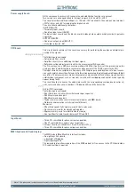
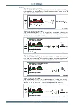
Note 1  The 37 protection is based on RMS value measurement of three phase currents (the computed RMS value takes into account the contribution 

of fundamental and harmonic up to eleventh order.)

Note 2  Starting of  

I<

def 

threshold takes place when at least one phase currents is undershot.

Note 3  Starting of 

I<<

def 

threshold takes place when all three phase currents are undershot.

Note 4  The 46N protection is based on INC neutral compensated current 

I

NC

 = I

N

 - I

C

 (I

N

 = RMS value of fundamental component for neutral current, 

I

C

 = compensation  setting for neutral current).

Note 5  Setting of  the compensation parameters are available inside the Set\46N Compensation menu, common for the A and B profi les  

‡

‡

‡

Summary of Contents for NC20

Page 1: ...NC20 Manual 01 2015 MANUAL NC20 MULTIFUNCTION PROTECTION FOR BANK CAPACITORS HARMONIC FILTERS WITH UNDER OVERVOLTAGE ELEMENTS...

Page 2: ...y Uaux 14 Phase current input circuits 14 Unbalance neutral current input circuit 14 Voltage input circuits 14 Binary input circuits 14 3 3 OUTPUT CIRCUITS 14 Relays 14 Block output Logic selectivity...

Page 3: ...rmal protection with RTD thermometric probes 26 48 Undervoltage 27 50 Undercurrent 37 54 TD Discharge time 56 Phase unbalance current 46 57 Neutral unbalance current 46N 63 Thermal image 49 71 Phase o...

Page 4: ...erse time curve IEC 60255 3 BS142 type C 171 Residual overcurrent 50N 51N Standard inverse time curve IEC 60255 3 BS142 type A 172 Residual overcurrent 50N 51N Very inverse time curve IEC 60255 3 BS14...

Page 5: ...on and commissioning must be carried out by quali ed person Thytronic assumes no re sponsibility for damages caused from improper use that does not comply all warning and caution in this manual In par...

Page 6: ...e nitions IEn Relay residual nominal current IEnp Residual CT primary nominal current In Relay phase nominal current Inp Phase CT primary nominal current INn Relay unbalance nominal current INnp Unbal...

Page 7: ...aracter istic quantity in reset condition is changed under speci ed condi tions and the instant when the relay operates Dropout ratio The ratio of a reset value to an operate value in well speci ed co...

Page 8: ...he 2nd threshold of the 50 element It is not available for reading missing arrow AND and NAND logic gates OR and NOR logic gates Limit block I threshold Computation block Max phase current Threshold s...

Page 9: ...FF Minimum pulse width operation for output relays tTR tTR t tTR INPUT OUTPUT tTR 0 T tTR t tTR INPUT OUTPUT Latched operating mode for output relays and LEDs Pulse operating mode for output relays t...

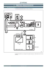
Page 10: ...nominal currents indepen dently selectable at 1 A or 5 A using dip switch Three phase voltages line to ground with nominal voltages programmable in the range 50 130 V UR 100V Two binary inputs One blo...

Page 11: ...witching type voltage stabilizing circuit having a very wide working range and a very small power dissipation Nominal frequency 50 or 60 Hz The most signi cant operating features are Programming of op...

Page 12: ...11 Voltage dips short interruptions and voltage variations on dc input power port immunity tests Interruption UT 40 100 ms Interruption UT 0 50 ms Voltage variations UT 80 120 10 s EMC tests for inter...

Page 13: ...mped oscillatory wave 1 MHz 30 A m Emission Reference standards EN 60255 25 IEC 60255 25 EN 61000 6 4 IEC 61000 6 4 EN 55011 CISPR 11 Electromagnetic emission tests Conducted emission auxiliary power...

Page 14: ...tral current input circuit Relay nominal unbalance nominal current INn 1 A or 5 A selectable by dip switch Permanent overload 25 A Thermal overload 1 s 500 A Dynamic overload half cycle 1250 A Rated c...

Page 15: ...yboard 8 keys 3 5 COMMUNICATION INTERFACES Local port Connection RJ10 Baud rate 19200 bps Parity None Protocol Modbus RTU Remote ports RS485 Connection screw terminals Baud rate 1200 57600 bps Protoco...

Page 16: ...dervoltage 27 Common con guration 27 Operating logic Logic27 AND OR U Element U Curve type U Curve DEFINITE INVERSE 3 De nite time 27 First threshold de nite time U def 0 05 1 10 Un step 0 01 Un U def...

Page 17: ...100 0 s step 0 1 s I2 Reset time delay t2 RES 0 00 100 0 s 0 00 9 99 s step 0 01 s 10 0 100 0 s step 0 1 s De nite time 46 Second threshold de nite time I2 def 1 150 step 1 I2 def within CLP I2CLP def...

Page 18: ...1 with 0 1 INn 1 with 1 INn Operate time accuracy 5 or 10 ms Thermal image 49 2 Common con guration Initial thermal image IN DthIN 0 0 1 0 B step 0 1 B Reduction factor at inrush KINR 1 0 3 0 step 0...

Page 19: ...10 00 In 0 100 0 999 In step 0 001 In 1 00 10 00 In step 0 01 In I inv within CLP ICLP inv 0 100 10 00 In 0 100 0 999 In step 0 001 In 1 00 10 00 In step 0 01 In I inv Operating time t inv 0 02 60 0 s...

Page 20: ...In 10 0 40 0 In step 0 1 In I def within CLP ICLP def 0 100 40 0 In 0 100 0 999 In step 0 001 In 1 00 9 99 In step 0 01 In 10 0 40 0 In step 0 1 In I def Operating time t def 0 03 10 00 s step 0 01 s...

Page 21: ...p 0 01 s 10 0 100 0 s step 0 1 s De nite time 50N 51N Third threshold de nite time IE def 0 100 40 0 In 0 100 0 999 In step 0 001 In 1 00 9 99 In step 0 01 In 10 0 40 0 In step 0 01 In IE def within C...

Page 22: ...Pickup time 0 03 s Dropout ratio 0 95 0 98 Dropout time 0 05 s Overshoot time 0 03 s Pickup accuracy 0 3 with0 1Un 0 1 with1Un Operate time accuracy 5 or 10 ms Breaker failure BF BF Phase current thr...

Page 23: ...Threshold S 0 10 0 95 step 0 01 74CT Overcurrent threshold I 0 10 1 00 In step 0 01 In S Operating time delay tS 0 03 200 s 0 03 9 99 s step 0 01 s 10 0 99 9 s step 0 1 s 100 200 s step 1 s Dropout r...

Page 24: ...rrent IN Calculated Thermal image DTheta Displacement angle of IN with respect to IL1 PhiN RMS value of fundamental component for compensated neutral current INC IN IC Displacement angle of INC with r...

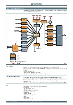
Page 25: ...Ram SRam SPI CPU ETHERNET CPU BOARD POWER SUPPLY BOARD INPUT MODULE DSP DUAL PORT 1A 5A EEprom Thybus RS485 RELAYS K1 K6 Output contacts RS232 MMI LCD LEDs BINARY INPUTS IN1 Input IN2 BLOCK I O BLKIN...

Page 26: ...ttainment of information pertaining to polarity and amplitude with high resolution The measurement criterion allows precise measurement of even those signals having a unidirectional component such as...

Page 27: ...cation protocol known as Basic Protocol BP Task The task process e thread are the base components Example are Keyboard management RTC Real Time Clock updating RAM EEPROM updating Diagnostic Input acqu...

Page 28: ...Basic Protocol BP manages the service communication between the kernel and the other modules through the communication buses with the following services Data and information exchange Calibration Upgra...

Page 29: ...ct measures of physical channels rst level Calculated measures second level Derived third level The measures concerning a level are based on data worked out in the previous level For each level the re...

Page 30: ...VT uL3 UL3 IL1 IL2 CT IL3 iL1 iL2 iL3 f T f T T F ai Hz Hz uL1 uL2 UL1 UL2 ACQUISITION VT uL3 UL3 IL1 IL2 CT IL3 iL1 iL2 iL3 f T f T IL1 ai In ACQUISITION iL1 iL2 iL3 DFT CT DFT DFT IL1 IL2 IL3 IL1 2...

Page 31: ...ai THDL1 THDL2 THDL3 IL1RMS IL1 THDL1 100 IL1RMS IL1 IL2RMS IL2 THDL2 100 IL2RMS IL2 IL3RMS IL3 THDL3 100 IL3RMS IL3 THD ai THDL1 THDL2 THDL3 IL1RMS IL1 THDL1 100 IL1RMS IL1 IL2RMS IL2 THDL2 100 IL2RM...

Page 32: ...mon parameter Fix Demand ai 1s IL1FIX IL2FIX IL3FIX tFIX In IL2 IL1 IL3 ILxFIX ILxn tFIX 60 tFIX 60 n 1 1 tFIX tFIX tFIX Fix Demand ai 1s IL1FIX IL2FIX IL3FIX tFIX In IL2 IL1 IL3 ILxFIX ILxn tFIX 60 t...

Page 33: ...ree phase rotating currents a direct cyclic sequence is de ned when the three phases are L1 L2 L3 ordered while an inverse cyclic sequence is de ned when the three phases are L1 L3 L2 ordered fasori a...

Page 34: ...urrent 50 51 g g g g g g g g Fundamental frequency phase overcurrent 50 51 g g g g g g g Residual overcurrent 50N 51N g g g g g g g Overvoltage 59 g g g g g Breaker failure BF g g g g g CONTROL MONITO...

Page 35: ...epresents the logical state of the binary input used in the following processing Each binary input may be matched to one of the following default functions FUNCTIONS Binary inputs IN1 IN2 Reset LEDs g...

Page 36: ...c INx tON Logic INx tOFF INx tOFF Binary input INx Reset led ai TRIPPING M ATRIX LED REL AYS Set ON turn on LED relay S Set Reset latch R Reset ON turn off LED relay Reset LEDs Binary input allocation...

Page 37: ...lock for Phase Block2 Iph and earth protective functions Block2 IE is similar to that illustrated in the scheme concerning the Block2 IphIIE Note 3 Unlike the Block2 selective block that houses a safe...

Page 38: ...TCS2 74TCS logic 74TCS logic Binary input INx T 0 IN1 tON 0 n o n c IN1 tON Logic IN1 tOFF IN1 tOFF Binary input INx T 0 IN1 tON 0 n o n c IN1 tON Logic IN1 tOFF IN1 tOFF TCS2 ai TRIP UAUX Trip Circui...

Page 39: ...Nx tON Logic INx tOFF IN2 tOFF Binary input allocation for CB remote command TRIPPING M ATRIX LED REL AYS UAUX UAUX 52a 52 O I 52b inhit theta ai t T ln Ith IB 2 D P D B Ith IB 2 1 2 D P D IN Binary i...

Page 40: ...until a reset command is issued RESET key ThySetter or communication command When pulse operating mode is set Operation MODE Pulse the output relay reset after a tTR programmable delay regardless of...

Page 41: ...g I Start relays I ST K g g g g g g I Trip relays I TR K g g g g g g IE Start relays IE ST K g g g g g g IE Trip relays IE TR K g g g g g g IE Start relays IE ST K g g g g g g IE Trip relays IE TR K...

Page 42: ...med with following operating mode No latched the LED reset at the end of the trip condition Latched the LED doesn t reset at the end of the trip condition it stays ON until a manual reset com mand is...

Page 43: ...g g I AL Trip LEDs I ALTR L g g g g g g g I Start LEDs I ST L g g g g g g g I Trip LEDs I TR L g g g g g g g I Start LEDs I ST L g g g g g g g I Trip LEDs I TR L g g g g g g g I Start LEDs I ST L g g...

Page 44: ...simple manner This is a con nection oriented transaction which means every query expects a response This query response technique ts well with the master slave nature of ModBus adding to the de termi...

Page 45: ...This nominal value must be set by means dip switch to 1 A or 5 A same as the secondary CT nomi nal current Dip switch is located on board of the CPU module the exhaustive treatment of Dip setup is de...

Page 46: ...l unbalance current when the primary measure ment reading mode is selected It must be programmed to the same value of the neutral CT s primary nominal current Es2 Un ai KTV V V 6000 3 100 3 60 Ung 6 0...

Page 47: ...s may be displayed according the following operating modes With RELATIVE setting all measures are related to the nominal value With PRIMARY setting all measures are related to the primary value Es1 IN...

Page 48: ...g localised overheating due to worn or non lubricated bearings The Pt100 probes detect the temperature in the range 50 C 250 C at 0 C its resistance is 100 ohm an alarm indicates any interruption or s...

Page 49: ...hALx Th x tThALx tTh x All alarm and or trip elements can be enabled or disabled by setting ON or OFF the ThALx Enable e Th x Enable parameters inside the Set Pro le A or B Thermal protection with RTD...

Page 50: ...tU inv 1 U U inv Where t operate time U relay input voltage U inv threshold setting tU inv operate time setting For the inverse time characteristic following data applies The operate time setting is r...

Page 51: ...nhibition U inhibition tU def tU inv U def tU def U def U inv U Curve U Enable State Block1 BLK1U U BLK1 Start U Block1 BLK1U U BLK1 Start U U BF Trip U U BF U AND U UL1 UL2 UL3 OR Common con guration...

Page 52: ...ING section Fun F27_S2 ai Logic diagram concerning the second threshold U of the undervoltage element 27 RESET tU def 0 T TRIPPING M ATRIX LED REL AYS tU def Start U Start U Trip U Trip U Trip U BF En...

Page 53: ...characteristic concerning the rst threshold U of the undervoltage element 27 0 9 0 1 1 U U inv 0 01 0 01 0 1 1 10 100 1000 10000 t s 0 25 tU inv 100 s tU inv 10 s tU inv 0 1 s tU inv 1 s t tU inv 1 U...

Page 54: ...and or I BLK1 enabling parameters are set to ON and a binary input is designed for logical block Block1 the protection is blocked off whenever the given input is active The trip timer is held in reset...

Page 55: ...ry input INx T 0 Logic INx tON INx tON INx tOFF T 0 n o n c INx tOFF State IL1RMS I def I def 37 Inhibition ON Inhibit by MMI Fun F37_S2 ai Logic diagram concerning the second threshold I of the under...

Page 56: ...ischarge time in seconds the initial value is the cor responding threshold set by TD decreased with resolution of 1 s to 0 When the discharge timer expires the display message is automatically removed...

Page 57: ...d if instead the current drops below the threshold the element is restored The element can be enabled or disabled by setting ON or OFF the the I2 Enable parameter inside the Set Pro le A or B Phase un...

Page 58: ...ed for output selective block Only when the committed pilot wire are used the continuity check of the pilot wire link is active Use of committed pilot wire input BLIN1 The protection is blocked off ac...

Page 59: ...e I2CLP def t2CLP TRIPPING M ATRIX LED REL AYS A B C A 1 A 0 or OFF Output t2CLP I2 Enable t2CLP CB State CB OPEN CB CLOSED CB OPEN Output t2CLP t 0 1 s HIGH THRESHOLD BLOCK LOW THRESHOLD UNBLOCK HIGH...

Page 60: ...2IN Iph Start I2 Trip I2 Iph Block2 IE Block2 BLK2IN IE tB timeout Block2 input tB K tB L Block1 FROM EARTH FAULT PROTECTIONS FROM ANY PROTECTIONS OFF ON IPh ON IPh IE ON IE BLIN1 Block1 T 0 tB IE Blo...

Page 61: ...I2CLP def t2CLP TRIPPING M ATRIX LED REL AYS A B C A 1 A 0 or OFF Output t2CLP I2 Enable t2CLP CB State CB OPEN CB CLOSED CB OPEN Output t2CLP t 0 1 s HIGH THRESHOLD BLOCK LOW THRESHOLD UNBLOCK HIGH...

Page 62: ...K2IN Iph Start I2 Trip I2 Iph Block2 IE Block2 BLK2IN IE tB timeout Block2 input tB K tB L Block1 FROM EARTH FAULT PROTECTIONS FROM ANY PROTECTIONS OFF ON IPh ON IPh IE ON IE BLIN1 Block1 T 0 tB IE Bl...

Page 63: ...parameters are adjustable inside the Set Compensation 46N menu The compensation may be performed Manually by means the Manual compensation command the setting IC and PhiC parameter are entered Automat...

Page 64: ...IN Element Setpoints menu Note 1 When the input value is more than 20 times the set point the operate time is limited to the value corresponding to 20 times the set point IC PhiC ACE Compensation 46N...

Page 65: ...is designed for logical block Block1 the concerning element is blocked off whenever the given input is active 2 The enabling parameters are available inside the Set Pro le A or B Neu tral unbalance c...

Page 66: ...et Pro le A or B Selective block BLOCK2 Selective block OUT menu 46NAL ai INC RESET tN ALdef 0 T 1 Start IN AL Trip I AL CB State ON Inhibit from IN and or IN element ON Enable IN AL unbalance current...

Page 67: ...CB CLOSED CB OPEN Output tNCLP t 0 1 s HIGH THRESHOLD BLOCK LOW THRESHOLD UNBLOCK HIGH THRESHOLD BLOCK A ON Change setting B OFF C ON Element blocking IN TR K IN TR L IN ST L IN ST K 1 CLP IN tN def t...

Page 68: ...tB L Block1 FROM EARTH FAULT PROTECTIONS FROM ANY PROTECTIONS OFF ON IPh ON IPh IE ON IE BLIN1 Block1 T 0 tB IE Block2 IE Block1 Block2 TRIPPING M ATRIX LED REL AYS 1 1 Neutral unbalance 46N Logic di...

Page 69: ...ED CB OPEN Output tNCLP t 0 1 s HIGH THRESHOLD BLOCK LOW THRESHOLD UNBLOCK HIGH THRESHOLD BLOCK A ON Change setting B OFF C ON Element blocking IN TR K IN TR L IN ST L IN ST K 1 CLP IN INC IN def IN d...

Page 70: ...tB L Block1 FROM EARTH FAULT PROTECTIONS FROM ANY PROTECTIONS OFF ON IPh ON IPh IE ON IE BLIN1 Block1 T 0 tB IE Block2 IE Block1 Block2 TRIPPING M ATRIX LED REL AYS 1 1 Neutral unbalance 46N Logic dia...

Page 71: ...rrent used for thermal image calculation is Ith max IL1 IL2 IL3 If the second harmonic restraint is enabled the thermal current used for thermal image calculation becomes Ith ILMAX KINR max IL1 IL2 IL...

Page 72: ...to ON The parameter is available inside the Set Pro le A or B Thermal image 49 Dth Element menu 3 Note 1 The CLP function Cold Load Pick up with blocking of the 49 element has priority compared with...

Page 73: ...for selective block Block2 the protection is blocked off by phase ele ments Block2 Iph or by any protection element Block2 Iph IE according the selectivity block criteria 2 The enable DthAL1BLK2IN Dt...

Page 74: ...tside CLP Pickup CLP setting change Block1 Block2 T 0 tDthCLP DthCLPMode tDthCLP Ith KINR TRIPPING M ATRIX LED REL AYS A B C A 1 A 0 or OFF Output tDthCLP DthAL1 Enable DThhAL1 thermal image 49 block...

Page 75: ...L Block1 FROM EARTH FAULT PROTECTIONS FROM ANY PROTECTIONS OFF ON IPh ON IPh IE ON IE BLIN1 Block1 T 0 tB IE Block2 IE 1 Block1 Block2 TRIPPING M ATRIX LED REL AYS 1 1 Block2 output ON Enable DthAL1BL...

Page 76: ...ide CLP Pickup CLP setting change Block1 Block2 T 0 tDthCLP DthCLPMode tDthCLP Ith KINR TRIPPING M ATRIX LED REL AYS A B C A 1 A 0 or OFF Output tDthCLP DthAL2 Enable DThhAL2 thermal image 49 block di...

Page 77: ...Block1 FROM EARTH FAULT PROTECTIONS FROM ANY PROTECTIONS OFF ON IPh ON IPh IE ON IE BLIN1 Block1 T 0 tB IE Block2 IE 1 Block1 Block2 TRIPPING M ATRIX LED REL AYS 1 1 Thermal image 49 Logic diagram of...

Page 78: ...BF Trip Dth TRIPPING M ATRIX LED REL AYS A B C A 1 A 0 or OFF Output tDthCLP Dth Enable DTh thermal image 49 block diagram tDthCLP CB State CB OPEN CB CLOSED CB OPEN Output tDthCLP t 0 1 s HIGH THRES...

Page 79: ...lock1 FROM EARTH FAULT PROTECTIONS FROM ANY PROTECTIONS OFF ON IPh ON IPh IE ON IE BLIN1 Block1 T 0 tB IE Block2 IE 1 Block1 Block2 TRIPPING M ATRIX LED REL AYS 1 1 Thermal image 49 Logic diagram of t...

Page 80: ...ual 01 2015 FUNCTION CHARACTERISTICS F_49 1min Char ai Operating characteristic concerning the thermal image element 49 T 1 min 1 1 1 2 3 4 5 6 7 8 9 10 20 Ith IB 0 01 0 1 1 10 100 1000 10000 1 0 p 0...

Page 81: ...01 2015 FUNCTION CHARACTERISTICS F_49 200min Char ai Operating characteristic concerning the thermal image element 49 T 200 min 1 1 1 2 3 4 5 6 7 8 9 10 20 Ith IB t s 0 1 1 10 100 1000 10000 100000 1...

Page 82: ...000 1 1 IRMS I inv 17 1 0 1 Where t operate time IRMS RMS input current I inv threshold setting t inv operate time setting The alarm threshold I AL has de nite time characteristic For all inverse time...

Page 83: ...adjustable time interval starting from the circuit breaker closure This operating mode may be select by setting ON Change setting the ICLP AL Mode and or ICLP Mode parameters whereas the operating thr...

Page 84: ...of committed pilot wire output BLOUT1 The information about phase or phase earth block may be select programming the ModeBLOUT1 parameter OFF ON IPh ON IPh IE ON IE inside Set Pro le A or B Selective...

Page 85: ...REL AYS A B C A 1 A 0 or OFF Output tCLP AL I AL Enable tCLP CB State CB OPEN CB CLOSED CB OPEN Output tCLP t 0 1 s HIGH THRESHOLD BLOCK LOW THRESHOLD UNBLOCK HIGH THRESHOLD BLOCK A ON Change setting...

Page 86: ...N Enable I BF towards BF logic I BF Trip I TRIPPING M ATRIX LED REL AYS I Curve 0 T A B C A 1 A 0 or OFF Output tCLP I Enable I overcurrent element 50 51RMS block diagram tCLP CB State CB OPEN CB CLOS...

Page 87: ...lock1 FROM EARTH FAULT PROTECTIONS FROM ANY PROTECTIONS OFF ON IPh ON IPh IE ON IE BLIN1 Block1 T 0 tB IE Block2 IE Block1 Block2 TRIPPING M ATRIX LED REL AYS 1 1 Phase overcurrent 50 51 RMS Logic dia...

Page 88: ...har ai 1 1 2 3 4 5 6 7 8 9 10 20 I RMS I inv 0 01 0 1 1 10 100 1000 10000 100000 1000000 t s t t inv 1 1 IRMS I inv 17 1 0 1 50000 t inv 0 1 s t inv 0 02 s t inv 1 0 s t inv 10 s t inv 60 s Operating...

Page 89: ...undamental I Element Setpoints menu The trip of I AL RMS element may be inhibited by the start of the second and or third element I I ofthefundamentalfrequencyphaseovercurrentbysettingONtheDisableI AL...

Page 90: ...lable Logical block Block1 If the I BLK1 and or I BLK1 enabling parameters are set to ON and a binary input is de signed for logical block Block1 the concerning element is blocked off whenever the giv...

Page 91: ...50 51 Fundamental I Element I Element Setpoints menus while the Block2 Iph and Block2 Iph IEfunctions must be assigned to the selected binary inputs inside the Set Inputs Binary input IN1 x menus IN1...

Page 92: ...ATRIX LED REL AYS A B C Output tCLP I Enable I overcurrent element 50 51 Fundamental Block diagram tCLP CB State CB OPEN CB CLOSED CB OPEN Output tCLP t 0 1 s HIGH THRESHOLD BLOCK LOW THRESHOLD UNBLO...

Page 93: ...FROM EARTH FAULT PROTECTIONS FROM ANY PROTECTIONS OFF ON IPh ON IPh IE ON IE BLIN1 Block1 T 0 tB IE Block2 IE 1 Block1 Block2 TRIPPING M ATRIX LED REL AYS 1 1 Phase overcurrent 50 51 Fundamental Logi...

Page 94: ...I overcurrent element 50 51 Fundamental Block diagram tCLP CB State CB OPEN CB CLOSED CB OPEN Output tCLP t 0 1 s HIGH THRESHOLD BLOCK LOW THRESHOLD UNBLOCK HIGH THRESHOLD BLOCK A ON Change setting B...

Page 95: ...1 FROM EARTH FAULT PROTECTIONS FROM ANY PROTECTIONS OFF ON IPh ON IPh IE ON IE BLIN1 Block1 T 0 tB IE Block2 IE 1 Block1 Block2 TRIPPING M ATRIX LED REL AYS 1 1 Phase overcurrent 50 51 Fundamental Log...

Page 96: ...023 Very Inverse ANSI IEEE type VI t tE inv 3 922 IEC IE inv 2 1 0 098 Extremely Inverse ANSI IEEE type EI t tE inv 5 64 IEC IE inv 2 1 0 024 Where t operate time IEC calculated residual current IE t...

Page 97: ...e menus For every of the four thresholds the following block criteria are available Logical block Block1 If the IE BLK1 IE BLK1 and or IE BLK1 enabling parameters are set to ON and a bi nary input is...

Page 98: ...f output relay K1 K6 If the IE BLK2OUT IE BLK2OUT and or IE BLK2OUT enable parameters are set to ONand a output relay is designed for selective block Block2 the protection issues a block output by pha...

Page 99: ...50N 51N IE inhibition BLK1IE IE BF IE Element Start IE Start IE Start IE Trip IE Trip IE IE disbyIE IE BLK2IN IE disbyIE BLK1IE IE Element BLK2OUT Start IE Start IE Trip IE IE disbyIE IE BLK1 IE BLK2...

Page 100: ...BF Trip IE TRIPPING M ATRIX LED REL AYS IE Curve 0 T A B C A 1 A 0 or OFF Output tECLP IE Enable IE residual overcurrent element 50 51 Block diagram tECLP CB State CB OPEN CB CLOSED CB OPEN Output tE...

Page 101: ...Block2 input tB K tB L Block1 FROM EARTH FAULT PROTECTIONS FROM ANY PROTECTIONS OFF ON IPh ON IPh IE ON IE BLIN1 Block1 T 0 tB IE Block2 IE Block1 Block2 TRIPPING M ATRIX LED REL AYS 1 1 Residual over...

Page 102: ...IE residual overcurrent element 50N 51N Block diagram tECLP CB State CB OPEN CB CLOSED CB OPEN Output tECLP t 0 1 s HIGH THRESHOLD BLOCK LOW THRESHOLD UNBLOCK HIGH THRESHOLD BLOCK A ON Change setting...

Page 103: ...lock1 FROM EARTH FAULT PROTECTIONS FROM ANY PROTECTIONS OFF ON IPh ON IPh IE ON IE BLIN1 Block1 T 0 tB IE Block2 IE Block1 Block2 TRIPPING M ATRIX LED REL AYS 1 1 Residual overcurrent 50N 51N Logic di...

Page 104: ...REL AYS A B C A ON Change setting B OFF C ON Element blocking Output tECLP IE Enable IE residual overcurrent element 50N 51N Block diagram tECLP CB State CB OPEN CB CLOSED CB OPEN Output tECLP t 0 1 s...

Page 105: ...Block1 FROM EARTH FAULT PROTECTIONS FROM ANY PROTECTIONS OFF ON IPh ON IPh IE ON IE BLIN1 Block1 T 0 tB IE Block2 IE Block1 Block2 TRIPPING M ATRIX LED REL AYS 1 1 Residual overcurrent 50N 51N Logic d...

Page 106: ...tting is referred to an input voltage equal to 1 5 of the pickup value Asymptotic reference value minimum pickup value 1 1 U inv Minimum operate time 0 1 s Range where the equation is valid 1 1 U U in...

Page 107: ...tment of the logical block Block 1 function may be found in the Logic Block paragraph inside CONTROL AND MONITOR ING section Fun F59_S1 ai U Curve 0 T RESET tU 0 T TRIPPING M ATRIX LED REL AYS tU def...

Page 108: ...e towards BF logic U BF Enable ON Enable Block1 input ON Block Block1 Block1 ON Inhibit U Inhibition U disbyU Binary input INx T 0 Logic INx tON INx tON INx tOFF T 0 n o n c INx tOFF U ST K U TR K U S...

Page 109: ...U inv 100 s t U inv 10 s t U inv 1 s t U inv 0 1 s 1 5 0 01 0 1 1 10 100 1000 10000 t s Inverse time operating characteristic concerning the rst threshold U of the overvoltage element 59 t tU inv U U...

Page 110: ...Set Pro le A or B Breaker failure BF menu All the IBF IEBF and tBF parameters can be set separately for Pro le A and Pro le B they are avail able inside the Set Pro le A or B Breaker failure BF menu B...

Page 111: ...ip BF Trip ProtExt 52a Block1 enable ON Enable BF BLK1 Block1 52a IBF Max IL1 IL3 IBF IL1 IL2 IL3 IEBF IE IEBF IE 1 RESET tBF 0 T tBF 1 Binary input INx T 0 Logic INx tON INx tON INx tOFF T 0 n o n c...

Page 112: ...lock it is not liable for any inhibition time out so the protective element is disabled for the whole time when the input is ON 2 Note 1 In the following treatment the logical block is de ned as Logic...

Page 113: ...ncerning the logic block element Block1 IE BLK1 50N 51N element IE BLK11 50N 51N element IE BLK1 50N 51N1 element U BLK1 59 element U BLK1 59 element 74TCSBLK1 74TCS element BFBLK1 BF element DthAL1BL...

Page 114: ...y an output block signal coming from a Pro N device or by a free voltage contact The protection is blocked off according the selectivity block criteria by phase elements Block2 Iph by earth elements B...

Page 115: ...tB Iph time related to the downstream relay does not take into account if such margin has been considered for the tF Iph setting s is a safety margin The chronometric selectivity applied among the tB...

Page 116: ...IE or phase earth ON IPh IE concerning the sending block out signal may be select by means of the ModeBLOUT1 parameter inside the Set Pro le A or B Selective block BLOCK2 Selective block OUT menu The...

Page 117: ...ing for a possible short circuit in the pilot wire or in the output circuit of the downstream protection The periodic pulses that are sent by output circuit may be enabled or disabled by means the Pul...

Page 118: ...the main circuit breaker CB1 by the A relay with a fault in 1 A Protection I element with de nite time set to 4 5 In with operate time to 0 10 s blocked by start of B and or C protection Settings I d...

Page 119: ...zero the Logic parameters ON OFF must be pro grammed in the same way of the related circuit connected with it The RemTrip K matching must be assigned to the selected output relays inside the Set Remot...

Page 120: ...tage is lower than 1 5 En the sampling frequency is xed to fn 50 or 60 Hz If the measured frequency is outside the locking range the sampling frequency is xed to the lower or upper value 45 or 55 Hz w...

Page 121: ...ecause it is likely that incorrect operation of the protection would occur on imbalance transient secondary current due to asymmetric line CTs saturation Depending upon the magnitude and duration of t...

Page 122: ...utput relays inside the Set CT supervision 74CT submenu the same for addressing the LED indicators S TR L If the S BLK1parameter is set to ON and a binary input is designed for logical block Block1 th...

Page 123: ...hen the input block goes down The 74TCS BLK1 parameter is available inside the Set Pro le A B Trip circuit supervision 74TCS submenu All the parameters can be set separately for Pro le A and Pro le B...

Page 124: ...r a 40 s delay in order to allow the fault clearing and the consequent reset of the TRIP protection Outputs are reset to zero after 6 s from the TRIP contact open 1 Note 1 The trip contact TRIP of the...

Page 125: ...To satisfy the above requirements the R value must be chosen between the Rmin and Rmax values typically the normalized value nearest the arithmetic mean R Rmin Rmax 2 The power dissipated by the R res...

Page 126: ...open K and CBclose K function must be set inside the Set Circuit breaker supervision LEDs relays allocation menu the CB position can be visualized by means two LEDs CBopen L and CBclosed L parameters...

Page 127: ...L TRIPPING M ATRIX LED REL AYS TRIPPING M ATRIX LED REL AYS TRIPPING M ATRIX LED REL AYS State N Open tbreak State SumI Opening transition N Open Mode N Open From CB position Opening transition Mode t...

Page 128: ...it information between protections installed in signi cant distance where the traditional connections are critical in terms of reliability Making OR logic for opening control of multiple DDI simultane...

Page 129: ...reset to zero by means the Reset on demand measures command Thysetter Commands menu The tROL Rolling demand period parameter is the same for rolling demand setting Oscillography Trigger Setup Followin...

Page 130: ...distortion factor for phase currents THDL1 THDL2 THDL3 THDL1 100 IL1 2 IL1 11th 2 IL1 100 IL1RMS IL1 THDL2 100 IL2 2 IL2 11th 2 IL2 100 IL2RMS IL1 THDL3 100 IL2 2 IL3 11th 2 IL3 100 IL3RMS IL1 RMS val...

Page 131: ...unters xx Start total counter xx I I 0 9999 xx Trip total counter xx I I 0 9999 xx Block1 total counter xx I I 0 9999 xx Block2 total counter xx I I 0 9999 Self test Lower level diagnostic MINOR can b...

Page 132: ...enabled for external selective block on output ST IE BLK2 ON OFF Phase protections output selective block state BLK2 OUT Iph ON OFF Ground protections output selective block state BLK2 OUT IE ON OFF P...

Page 133: ...ages uL1 uL2 uL3 Analog channels RMS value for phase currents IL1RMS IL2RMS IL3RMS Fundamental component for phase currents IL1 IL2 IL3 Fundamental component for input voltages UL1 UL2 UL3 Fundamental...

Page 134: ...IL3RMS IN Logic variables K1 K2 K3 K4 K5 K6 IN1 IN2 up to 116 record can be stored if f 50 Hz since Example 2 With following setting Pre trigger 0 5 s Post trigger 0 5 s Sampled data iL1 iL2 iL3 iE An...

Page 135: ...tection availability Flush mounting The xed case tted with special fastening brackets is mounted on the front of electric control board previously drilled as indicated in the drawing In case of side b...

Page 136: ...ing distance is determined by the dimensions of the mounting plate indicated in the overall dimensions drawing increased horizontally and vertically by as much as needed to allow room for the wiring a...

Page 137: ...rate mount ai Separate operator panel F1 D1 RX TX F2 F3 F4 F5 A1 A2 A3 A4 A5 A6 A7 A8 A9 A10 A11 A12 A13 A14 A15 A16 A17 A18 A19 A20 A21 A22 B1 B2 B3 B4 B5 B6 B7 B8 C1 C2 C4 C3 C5 C6 C7 C8 E1 128 5 11...

Page 138: ...r a one unit space must be provided when several rack are overlapping mounted Rack mount ai Rack mounting 177 4U 101 6 482 6 465 ON 4 1 3 2 5 TRIP START ON 4 1 3 2 5 TRIP START ON 4 1 3 2 5 TRIP START...

Page 139: ...torque 0 5 0 6 Nm Stripping length 10 mm The connections to the current signal inputs C1 C8 can be made by ring lugs and an insulating panel covering the terminals may be mounted for safety purposes...

Page 140: ...voltage of the control panel The inputs are polarity free with wide voltage range The optoisolated inputs are immune to transitory interferences however the following recommenda tion must be considere...

Page 141: ...must be employed if an FX port is implemented The link must be enabled by means ThySetter sw and RS232 connection Set the IP address Host IP address e IP net mask in order that the NA10 and PC paramet...

Page 142: ...ce of the induc tive components of the same which might compromise good communication RS485 120 SUPERVISION UNIT OUTPUT RELAYS UAUX A1 A2 A9 A10 A11 A12 A13 A14 E1 THYBUS D1 ETHERNET A3 A4 A5 A6 A7 A8...

Page 143: ...PT100 PT100 MODULE INPUT PT2 MPT2 PT3 MPT3 PT4 MPT4 PT8 MPT8 PT7 MPT7 PT6 MPT6 PT5 MPT5 PUT N I S U B Y H T T U P T U O S U B Y H T MPT 8 T1 PT1 PT8 MPT1 MPT8 PT7 MPT7 PT6 MPT6 PT5 MPT5 PT2 MPT2 PT3...

Page 144: ...re installed the hardware address must be set to avoid communication collisions on the Thybus for this purpose the default address must be changed on one module by means of dip switch on the top circu...

Page 145: ...s example they cannot be comprehensive for real applications Block sch ai Logic selectivity with BFO BLIN1 BLIN1 BLIN1 Block2 IPh BLOUT1 BLOUT1 TRIP I TRIP I TRIP I TRIP I Any device Block sch ai Logi...

Page 146: ...power supply before extracting or re inserting the relay If an attempting is made to insert a relay into an un matching case a mechanical code will prevent full insertion Demage can result if excessiv...

Page 147: ...g screw in order avoid loss of the internal wash er Unmounting of the case from the switchboard is not needed Split the MMI module and disconnect cable set in ai Unmounting set in ai Unmounting Split...

Page 148: ...ular attention to avoid any accidental contact with the internal components In order to avoid the static electricity accumulated in the human body from causing damage it is recommended to observe the...

Page 149: ...the CPU board Facory defaul settings In 5 A phase currents INn 1 A unbalanced neutral current set in ai ETHERNET THYBUS 1 A 5 A S5 485 1 2 3 4 IL1 IL2 IL3 IN Dip switch setting inside the CPU board Fa...

Page 150: ...art information of any protective functions LED TRIP red committed for trip information of any protective functions 6 6 FINAL OPERATIONS Before energizing the electric board it is advisable to check t...

Page 151: ...e Products Software 1 ThySetter use Please refer to ThySetter user manual for detailed instructions The document is available on www thytronic it Product Sotware ThySetter Download area Note 1 Startin...

Page 152: ...reaker Close command At power up the display shows the text THYTRONIC PRO NC20 xxx x serial number date and time 01 01 2000 00 00 The ON green Led points out the auxiliary power supply voltage permane...

Page 153: ...e auxiliary power supply to the NC20 relay As example to set the operating mode of the K1 output relay as ENERGIZED LATCHED the following procedure must be issued By means Down button select the Set m...

Page 154: ...he RS485 Protocol or Ethernet parameters message to enter you must press the Right button As example to select the address 12 for the ModBus protocol the following procedure must be issued Select the...

Page 155: ...menu command Communication Open Verify that inside the modality box Serial and Automatic are selected Thysetter will search automatically the relay from the template regardless of what is selected in...

Page 156: ...r about 3 minutes elapsed without pressing any button If you do not want to wait three minutes of waiting it must go back to the password menu and come out without input any data and until the the mes...

Page 157: ...IE OFF CLP IE OFF BLK1 IE OFF BLK2IN IE OFF BLK4IN IE OFF Start IE OFF Trip IE OFF CLP IE OFF BLK1 IE OFF BLK2IN IE OFF BLK4IN IE OFF Start IE OFF Trip IE OFF CLP IE OFF BLK1 IE OFF BLK2IN IE OFF BLK...

Page 158: ...2Dth cnt 0 ParTrDth cnt 0 ParBk1Dth cnt 0 ParBk1BFcnt 0 ParStBFcnt 0 ParTrTrcnt 0 ParBk1 74TCScnt 0 ParTr74TCScnt 0 ParBk1 74CTcnt 0 ParTr74CTcnt 0 ParBk1IE cnt 0 ParTrIE cnt 0 ParStIE cnt 0 ParStIE c...

Page 159: ...Operating phase IL2r 0 In IL1rms r 0 In Fault 0 Cause Date Time IL2rms r 0 In IL3rms r 0 In IL3r 0 In UL2r 0 Un UL1r 0 Un UL3r 0 Un IECr 0 In INCr 0 INn I2r 0 INr 0 INn PhiNr 0 gr PhiNCr 0 gr DTheta r...

Page 160: ...TD TD Enable OFF tD 1 min Relays TD TD K LEDs TD TD L 37 I Element I Element I Enable OFF I def enable OFF I def 0 5 In t def 1 s I BLK1 OFF I BF OFF Relays I I TR K I ST K I ST L I TR L LEDs I I def...

Page 161: ...NU PROCEED PROFILE A MENU 49 DthAL1 Element Common DthAL2 Element Dth Element DthIN 0 DThetaB KINR 2 T 10 min DthCLP Mode OFF DthCLP 0 1 s DthAL1 Enable OFF DthAL1 0 5 DthetaB DthAL1BLK1 OFF DthAL1BLK...

Page 162: ...K2OUT OFF IE BLK2IN OFF IE BF OFF IE Curve DEFINITE Relays IE IE TR K IE ST K IE ST L IE TR L LEDs IE tECLP 0 1 s tE RES 0 s IE def enable OFF IECLP def 2 IEn IE Enable OFF IECLP Mode OFF tE def 1 s I...

Page 163: ...WIRE DIAGNOSTIC PulseBLOUT1 OFF PulseBLIN1 OFF N ROL 12 tRoll 5 min DEMAND MEASURES Periods tFix 15 min BF IEBF 0 1 IEn IBF 0 1 In IBF enable ON IEBF enable ON BF Enable OFF CB Input ON BF BLK1 OFF t...

Page 164: ...nt values referred to the nominal current of the current transformers as directly in primary amperes according to the preset value of CT s nominal primary current the same is done for the input voltag...

Page 165: ...racteristics following data applies Asymptotic reference value minimum pickup value 1 1 I inv Minimum operate time 0 1 s Range where the equation is valid 2 3 1 1 I I inv 20 If I pickup 2 5 In the upp...

Page 166: ...BS142 type A F_46N IECA Char ai 1 1 2 3 4 5 6 7 8 9 10 20 I NC IN inv 0 01 0 1 1 10 100 1000 10000 t s tN inv 10 s tN inv 60 s tN inv 5 s tN inv 1 s tN inv 0 5 s tN inv 0 2 s tN inv 0 1 s tN inv 0 02...

Page 167: ...BS142 type B F_46N IECB Char ai 1 1 2 3 4 5 6 7 8 9 10 20 INC IN inv 0 01 0 1 1 10 100 1000 10000 t s tN inv 10 s tN inv 60 s tN inv 5 s tN inv 1 s tN inv 0 5 s tN inv 0 2 s t inv 0 02 s t inv 0 1 s 1...

Page 168: ...5 3 BS142 type C F_51 IECC Char ai 1 1 2 3 4 5 6 7 8 9 10 20 INC IN inv 0 01 0 1 1 10 100 1000 10000 100000 t s tN inv 10 s tN inv 60 s tN inv 5 s tN inv 1 s t inv 0 5 s t inv 0 2 s t inv 0 02 s t inv...

Page 169: ...3 BS142 type A F_51 IECA Char ai 1 1 2 3 4 5 6 7 8 9 10 20 I RMS I inv 0 01 0 1 1 10 100 1000 10000 t s t inv 10 s t inv 60 s t inv 5 s t inv 1 s t inv 0 5 s t inv 0 2 s t inv 0 1 s t inv 0 02 s t t i...

Page 170: ...55 3 BS142 type B F_51 IECB Char ai 1 1 2 3 4 5 6 7 8 9 10 20 IRMS I inv 0 01 0 1 1 10 100 1000 10000 t s t inv 10 s t inv 60 s t inv 5 s t inv 1 s t inv 0 5 s t inv 0 2 s t inv 0 02 s t inv 0 1 s 13...

Page 171: ...3 BS142 type C F_51 IECC Char ai 1 1 2 3 4 5 6 7 8 9 10 20 IRMS I inv 0 01 0 1 1 10 100 1000 10000 100000 t s t inv 10 s t inv 60 s t inv 5 s t inv 1 s t inv 0 5 s t inv 0 2 s t inv 0 02 s t inv 0 1...

Page 172: ...BS142 type A F_51N IECA Char ai 1 1 2 3 4 5 6 7 8 9 10 20 IEC IE inv 0 01 0 1 1 10 100 1000 10000 t s tE inv 10 s tE inv 60 s tE inv 5 s tE inv 1 s tE inv 0 5 s tE inv 0 2 s tE inv 0 1 s tE inv 0 02 s...

Page 173: ...142 type B F_51N IECB Char ai 1 1 2 3 4 5 6 7 8 9 10 20 I EC IE inv 0 01 0 1 1 10 100 1000 10000 t s tE inv 10 s tE inv 60 s tE inv 5 s tE inv 1 s tE inv 0 5 s tE inv 0 2 s tE inv 0 02 s tE inv 0 1 s...

Page 174: ...3 BS142 type C F_51 IECC Char ai 1 1 2 3 4 5 6 7 8 9 10 20 IE IE inv 0 01 0 1 1 10 100 1000 10000 100000 t s tE inv 10 s tE inv 60 s tE inv 5 s tE inv 1 s tE inv 0 5 s tE inv 0 2 s tE inv 0 02 s tE in...

Page 175: ...rve L 0 024 for ANSI IEEE Extremely inverse curve For all inverse time characteristics following data applies Asymptotic reference value minimum pickup value 1 1 I inv Minimum operate time 0 1 s Range...

Page 176: ...type MI F_46N ANSIMI Char ai 1 1 2 3 4 5 6 7 8 9 10 20 INC IN inv 0 01 0 1 1 10 100 1000 10000 t s tN inv 10 s tN inv 60 s tN inv 5 s tN inv 1 s t inv 0 02 s t inv 0 2 s t inv 0 1 s t inv 0 5 s t tN i...

Page 177: ...VI F_46N ANSIVI Char ai 1 1 2 3 4 5 6 7 8 9 10 20 INC IN inv 0 01 0 1 1 10 100 1000 10000 t s tN inv 10 s tN inv 60 s tN inv 5 s tN inv 1 s t inv 0 5 s t inv 0 2 s t inv 0 1 s t inv 0 02 s t tN inv I...

Page 178: ...E type EI F_46N ANSIEI Char ai 1 1 2 3 4 5 6 7 8 9 10 20 INC IN inv 0 01 0 1 1 10 100 1000 10000 t s tN inv 10 s tN inv 60 s tN inv 5 s t inv 0 5 s t inv 1 s t inv 0 2 s t inv 0 1 s t inv 0 02 s t tN...

Page 179: ...type MI F_51 ANSIMI Char ai 1 1 2 3 4 5 6 7 8 9 10 20 IRMS I inv 0 01 0 1 1 10 100 1000 10000 t s t inv 10 s t inv 60 s t inv 5 s t inv 1 s t inv 0 02 s t inv 0 2 s t inv 0 1 s t inv 0 5 s t t inv IRM...

Page 180: ...type VI F_51 ANSIVI Char ai 1 1 2 3 4 5 6 7 8 9 10 20 IRMS I inv 0 01 0 1 1 10 100 1000 10000 t s t inv 10 s t inv 60 s t inv 5 s t inv 1 s t inv 0 5 s t inv 0 2 s t inv 0 1 s t inv 0 02 s t t inv IRM...

Page 181: ...type EI F_51 ANSIEI Char ai 1 1 2 3 4 5 6 7 8 9 10 20 IRMS I inv 0 01 0 1 1 10 100 1000 10000 t s t inv 10 s t inv 60 s t inv 5 s t inv 0 5 s t inv 1 s t inv 0 2 s t inv 0 1 s t inv 0 02 s t t inv IR...

Page 182: ...pe MI F_51N ANSIMI Char ai 1 1 2 3 4 5 6 7 8 9 10 20 IEC IE inv 0 01 0 1 1 10 100 1000 10000 t s tE inv 10 s tE inv 60 s tE inv 5 s tE inv 1 s tE inv 0 02 s tE inv 0 2 s tE inv 0 1 s tE inv 0 5 s t tE...

Page 183: ...I F_51N ANSIVI Char ai 1 1 2 3 4 5 6 7 8 9 10 20 IEC IE inv 0 01 0 1 1 10 100 1000 10000 t s tE inv 10 s tE inv 60 s tE inv 5 s tE inv 1 s tE inv 0 5 s tE inv 0 2 s tE inv 0 1 s tE inv 0 02 s t tE inv...

Page 184: ...ype EI F_51N ANSIEI Char ai 1 1 2 3 4 5 6 7 8 9 10 20 IEC IE inv 0 01 0 1 1 10 100 1000 10000 t s tE inv 10 s tE inv 60 s tE inv 5 s tE inv 0 5 s tE inv 1 s tE inv 0 2 s tE inv 0 1 s tE inv 0 02 s t t...

Page 185: ...ERNET RS485 F1 F2 F3 F4 F5 A B OUTPUT RELAYS A9 A10 A11 A12 A13 A14 A3 A4 A5 A6 A7 A8 K2 K3 K4 K5 K6 K1 BLOCK OUT A15 BLOUT BLOUT A16 BLOCK IN A17 A18 C1 IL1 IL2 IL3 CURRENT INPUTS C2 C3 C4 C5 C6 IN C...

Page 186: ...TPUT MPT ON BUS RUN MODULO PT100 PT100 MODULE INPUT OUTPUT MID16 ON BUS RUN MODULO INGRESSI REMOTI INPUT 34 36 35 30 32 33 31 28 29 43 44 45 39 40 42 41 38 37 52 54 53 48 50 51 49 46 47 1 2 3 4 5 6 7...

Page 187: ...cannot be comprehensive for real applications For all diagrams the output contacts are shown in de energized state for standard reference NC20 sch1 ai NC20 L1 L2 L3 A B A B a b a b IN C7 C8 P2 P1 S1 S...

Page 188: ...PPENDIX NC20 sch2 ai NC20 L1 L2 L3 A B A B a b a b IN C7 C8 P2 P1 S1 S2 UL1 UL2 UL3 B6 B3 B4 B5 B1 B2 27 59 46 49 37 50 51 50 51 RMS 74CT 46N BINARY INPUTS 50BF CB position Two phase CTs C2 C1 C3 C4 C...

Page 189: ...5 C6 C7 C8 E1 128 5 110 200 168 20 205 149 30 5 30 107 177 4 5 102 5 0 3 70 161 154 4 5 4 5 212 5 25 15 170 275 177 4U 101 6 482 6 465 RACK MOUNTING FLUSH MOUNTING CUTOUT SIDE VIEWS FRONT VIEWS ON 4 1...

Page 190: ...ements reading mode RELATIVE PRIMARY Language English Turkish Russian Inputs Binary input IN1 IN1 Logic Active ON Active OFF IN1 tON Value s 0 00 9 99 step 0 01 10 0 100 0 step 0 1 IN1 tOFF Value s 0...

Page 191: ...tched TRIP Type No latched Latched L1 Type No latched Latched L2 Type No latched Latched L3 Type No latched Latched L4 Type No latched Latched L5 Type No latched Latched L6 Type No latched Latched Typ...

Page 192: ...rm NO YES Self test relay K1 K2 K3 K4 K5 K6 K7 K8 K9 K10 MMI Display modules Assigned modules All modules 46N Compensation Compensation current IC INn 0 00 0 50 step 0 01 Compensation angle PhiC deg 0...

Page 193: ...Th 3 Enable OFF ON 26 PT3 Trip threshold Th 3 C 0 200 step 1 Th 3 Operating time Value s 0 100 step 1 Th 3 Breaker failure Th 3BF OFF ON Th 3 Trip relays Th 3 K K1 K2 K3 K4 K5 K6 K7 K8 K9 K10 Th 3 Tri...

Page 194: ...1 Th 6 Operating time Value s 0 100 step 1 Th 6 Breaker failure Th 6BF OFF ON Th 6 Trip relays Th 6 K K1 K2 K3 K4 K5 K6 K7 K8 K9 K10 Th 6 Trip LEDs Th 6 L START TRIP L1 L2 L3 L4 L5 L6 L7 L8 L9 L10 PT7...

Page 195: ...ST K K1 K2 K3 K4 K5 K6 K7 K8 K9 K10 U Trip relays U TR K K1 K2 K3 K4 K5 K6 K7 K8 K9 K10 U Start LEDs U ST L START TRIP L1 L2 L3 L4 L5 L6 L7 L8 L9 L10 U Trip LEDs U TR L START TRIP L1 L2 L3 L4 L5 L6 L...

Page 196: ...K5 K6 K7 K8 K9 K10 I Trip relays I TR K K1 K2 K3 K4 K5 K6 K7 K8 K9 K10 I Start LEDs I ST L START TRIP L1 L2 L3 L4 L5 L6 L7 L8 L9 L10 I Trip LEDs I TR L START TRIP L1 L2 L3 L4 L5 L6 L7 L8 L9 L10 De ni...

Page 197: ...p 0 01 10 0 100 0 step 0 1 I2 Logical block I2 BLK1 OFF ON I2 Input selective block I2 BLK2IN OFF ON I2 Output selective block I2 BLK2OUT OFF ON I2 Breaker failure I2 BF OFF ON I2 Disabling by I2 star...

Page 198: ...IN Output selective block IN BLK2OUT OFF ON IN Breaker failure IN BF OFF ON IN AL Disabling by IN IN ALdisbyIN OFF ON IN Start relays IN ST K K1 K2 K3 K4 K5 K6 K7 K8 K9 K10 IN Trip relays IN TR K K1 K...

Page 199: ...Mode OFF ON Element blocking ON Change setting DthCLP Activation time Value s 0 00 9 99 step 0 01 10 0 100 0 step 0 1 DthAL1 Element DthAL1 Enable DthAL1 Enable OFF ON 49 First alarm threshold DthAL1...

Page 200: ...ON Pickup value In 0 100 0 999 step 0 001 1 00 10 00 step 0 01 I ALdef within CLP ICLP ALdef In 0 100 0 999 step 0 001 1 00 10 00 step 0 01 I ALdef Operating time Value s 0 03 9 99 step 0 01 10 0 99...

Page 201: ...0 0 step 0 1 I Reset time delay Value s 0 00 9 99 step 0 01 10 0 100 0 step 0 1 I Logical block I BLK1 OFF ON I Input selective block I BLK2IN OFF ON I Output selective block I BLK2OUT OFF ON I Breake...

Page 202: ...001 1 00 9 99 step 0 01 10 0 40 0 step 0 1 I def Operating time Value s 0 03 10 00 step 0 01 Residual overcurrent 50N 51N IE Element Setpoints IE Enable IE Enable OFF ON IE Curve type IE Curve IEC BS...

Page 203: ...ective block IE BLK2OUT OFF ON IE Breaker failure IE BF OFF ON IE Disabling by IE start IE disbyIE OFF ON IE Start relays IE ST K K1 K2 K3 K4 K5 K6 K7 K8 K9 K10 IE Trip relays IE TR K K1 K2 K3 K4 K5 K...

Page 204: ...mon con guration 59 Operating logic Logic59 OR AND U Element Setpoints U Enable U Enable OFF ON U Curve type U Curve INVERSE DEFINITE U Logical block U BLK1 OFF ON U Breaker failure U BF OFF ON U Star...

Page 205: ...lays tB K K1 K2 K3 K4 K5 K6 K7 K8 K9 K10 tB Iph IE Elapsed signalling LEDs tB L START TRIP L1 L2 L3 L4 L5 L6 L7 L8 L9 L10 Selective block OUT BLOUT1 Selective block operating mode ModeBLOUT1 OFF ON IP...

Page 206: ...8 L9 L10 Th 1 Trip Th 1 Enable Th 1 Enable OFF ON 26 PT1 Trip threshold Th 1 C 0 200 step 1 Th 1 Operating time Value s 0 100 step 1 Th 1 Breaker failure Th 1BF OFF ON Th 1 Trip relays Th 1 K K1 K2 K3...

Page 207: ...4 Operating time Value s 0 100 step 1 Th 4 Breaker failure Th 4BF OFF ON Th 4 Trip relays Th 4 K K1 K2 K3 K4 K5 K6 K7 K8 K9 K10 Th 4 Trip LEDs Th 4 L START TRIP L1 L2 L3 L4 L5 L6 L7 L8 L9 L10 PT5 Pro...

Page 208: ...ure Th 7BF OFF ON Th 7 Trip relays Th 7 K K1 K2 K3 K4 K5 K6 K7 K8 K9 K10 Th 7 Trip LEDs Th 7 L START TRIP L1 L2 L3 L4 L5 L6 L7 L8 L9 L10 PT8 Probe ThAL8 Alarm ThAL8 Enable ThAL8 Enable OFF ON 26 PT8 A...

Page 209: ...block U BLK1 OFF ON U Breaker failure U BF OFF ON U Disabling by U start U disbyU OFF ON U Start relays U ST K K1 K2 K3 K4 K5 K6 K7 K8 K9 K10 U Trip relays U TR K K1 K2 K3 K4 K5 K6 K7 K8 K9 K10 U Star...

Page 210: ...L6 L7 L8 L9 L10 Phase unbalance 46 I2 Element Setpoints I2 Enable I2 Enable OFF ON I2CLP Mode I2CLP Mode OFF ON Element blocking ON Change setting I2CLP Activation time Value s 0 00 9 99 step 0 01 10...

Page 211: ...05 9 99 step 0 01 10 0 60 0 step 0 1 Neutral unbalance current 46N IN AL Element Setpoints IN AL Enable IN AL Enable OFF ON INCLP AL Mode INCLP AL Mode OFF ON Element blocking ON Change setting INCLP...

Page 212: ...State OFF ON Pickup value INn 0 01 1 00 step 0 01 IN inv within CLP INCLP inv INn 0 01 1 00 step 0 01 IN inv Operating time tN inv s 0 02 9 99 step 0 01 10 0 60 0 step 0 1 IN Element Setpoints IN Enab...

Page 213: ...2 Input selective block DthAL2BLK2IN OFF ON DthAL2 Output selective block DthAL2BLK2OUT OFF ON DthAL2 Alarm relays DthAL2 K K1 K2 K3 K4 K5 K6 K7 K8 K9 K10 DthAL2 Alarm LEDs DthAL2 L START TRIP L1 L2 L...

Page 214: ...lective block I BLK2IN OFF ON I Output selective block I BLK2OUT OFF ON I Breaker failure I BF OFF ON I AL Disabling by I I ALdisbyI OFF ON I Start relays I ST K K1 K2 K3 K4 K5 K6 K7 K8 K9 K10 I Trip...

Page 215: ...ON Pickup value In 0 100 0 999 step 0 001 1 00 9 99 step 0 01 10 0 40 0 step 0 1 I def within CLP ICLP def In 0 100 0 999 step 0 001 1 00 9 99 step 0 01 10 0 40 0 step 0 1 I def Operating time Value s...

Page 216: ...F ON IE Breaker failure IE BF OFF ON IE Start relays IE ST K K1 K2 K3 K4 K5 K6 K7 K8 K9 K10 IE Trip relays IE TR K K1 K2 K3 K4 K5 K6 K7 K8 K9 K10 IE Start LEDs IE ST L START TRIP L1 L2 L3 L4 L5 L6 L7...

Page 217: ...me Value s 0 03 10 00 step 0 01 IE Element Setpoints IE Enable IE Enable OFF ON IECLP Mode IECLP Mode OFF ON Element blocking ON Change setting IECLP Activation time Value s 0 00 9 99 step 0 01 10 0 1...

Page 218: ...Un 0 50 1 50 step 0 01 U inv Operating time tU inv s 0 10 9 99 step 0 01 10 0 100 0 step 0 1 U Element Setpoints U Logical block U BLK1 OFF ON U Breaker failure U BF OFF ON U Disabling by U start U di...

Page 219: ...K6 K7 K8 K9 K10 Phase and ground protections output selective block relays BLK2OUT Iph IE K K1 K2 K3 K4 K5 K6 K7 K8 K9 K10 Phase protections output selective block LEDs BLK2OUT Iph L START TRIP L1 L2...

Page 220: ...6 27 28 29 30 31 32 33 34 35 36 37 38 39 40 41 42 43 44 45 46 47 48 49 50 51 52 53 54 55 56 57 58 59 60 61 62 63 64 65 66 67 68 69 70 71 72 73 74 75 76 77 78 79 80 81 82 83 84 85 86 87 88 89 90 91 92...

Page 221: ...mer 6 s 0 00 0 99 step 0 01 1 0 60 0 step 0 1 Timer 7 s 0 00 0 99 step 0 01 1 0 60 0 step 0 1 Timer 8 s 0 00 0 99 step 0 01 1 0 60 0 step 0 1 Timer 9 s 0 0 59 9 step 0 1 60 299 step 1 300 3600 step 10...

Page 222: ...ipping I 2t threshold SumI 2t In 2s 0 5000 step 1 CB operating time mode Mode tOpen OFF ON Trigger relay for CB opening time trigger measurement Ktrig break K1 K2 K3 K4 K5 K6 K7 K8 K9 K10 Circuit brea...

Page 223: ...e Trigger Stopped Wait Fail Off Records 0 0 step 0 Buffer storage 0 0 step 0 Trigger Setup Pre trigger time s 0 05 1 00 step 0 01 Post trigger time s 0 05 60 00 step 0 05 Element pickup trigger ON OFF...

Page 224: ...uency IL1rms IL1 UL1 IL2rms IL2 UL2 IL3rms IL3 UL3 IN PhiN INC PhiNC IEC I2 T1 T2 T3 T4 T5 T6 T7 T8 Off Set digital channels Binary 1 K1 K2 K3 K4 K5 K6 K7 K8 K9 K10 IN1 IN2 Off Binary 2 K1 K2 K3 K4 K5...

Page 225: ...irobi S Petersburg UTC 4 Baku Dubai Mauritius Samara Tbilisi UTC 5 Karachi Maldives Tashkent Yekaterinburg UTC 6 Almaty Dhaka Omsk UTC 1 Azores CapoVerde UTC 2 Mid Atlantic UTC 3 Brasilia Bueno sAires...

Page 226: ...ThySetter 3 6 9 ThySetter 3 6 11 18 03 2013 11 2013 03 2014 01 2015 First edition PLC description 26 element ThySetter description removed dedicated manual Current inputs burden output relays breaking...

Page 227: ...ctive EMC Directive Reference of standards and or technical speci cations applied for this declaration of conformity or parts thereof harmonized standards Reference n Issue Title EN 61010 1 EN 50263 E...

Reviews: