

73
NC20 - Manual - 01 - 2015
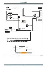
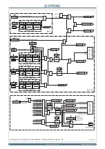
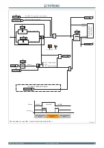
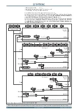
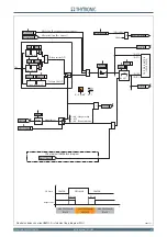
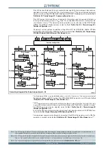
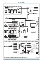
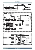
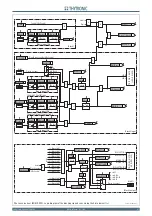
FUNCTION CHARACTERISTICS
For every threshold the following block criteria are available:
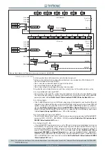
Logical block (Block1)
If the
DthAL1BLK1, DthAL2BLK1
and/or
Dth>BLK1
enabling parameters are set to
ON
and a bi-
nary input is designed for logical block (Block1), the concerning element is blocked off whenever the
given input is active.
[1]
The enabling parameters are available inside the
Set \ Profi le A(or B) \Ther-
mal image-49 \ DthAL1 Element
(
DthAL2 Element
,
Dth> Element)
menus, while the
Block1
function
must be assigned to the selected binary input inside the
Set \ Inputs \ Binary input IN1(x)
menus.
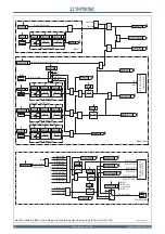
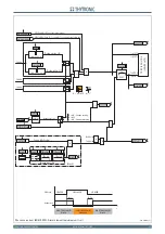
Selective block (Block2)
All along the protective elements the selective block may be set.
The logic selectivity function may be performed by means any combination of the following I/O:
One committed pilot wire input (BLIN1).
One or more binary inputs designed for input selective block.
One committed pilot wire output (BLOUT1).
One or more output relays designed for output selective block.
Only when the committed pilot wire are used the continuity check of the pilot wire link is active.
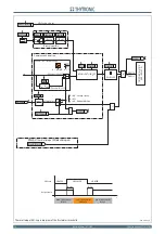
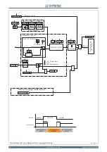
Use of committed pilot wire input BLIN1:
The protection is blocked off according the selectivity block criteria when the input BLIN1 is active.
The information about phase or phase+earth block may be select programming the
ModeBLIN1
parameter inside the
Set \ Profi le A(or B) \ Selective block-BLOCK2 \ Selective block IN
menus.
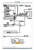
Use of binary inputs:
If the
DthAL1BLK2IN, DthAL2BLK2IN
and/or
Dth>BLK2IN
parameter are are set to
ON
and
a binary input is designed for selective block (Block2), the protection is blocked off by phase ele-
ments (Block2 Iph) or by any protection element (Block2 Iph/IE) according the selectivity block
criteria.
[2]
The enable
DthAL1BLK2IN, DthAL2BLK2IN
and/or
Dth>BLK2IN
parameters are
available inside the
Set \ Profi le A(or B) \ Thermal image-49 \
DthAL1 Element
,
DthAL2 Element
,
Dth> Element
menus, while the
Block2 Iph
and
Block2 Iph/IE
functions must be assigned to the
selected binary inputs inside the
Set \ Inputs \ Binary input IN1(2)
menus (IN1 or IN2 matching).
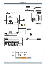
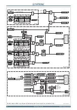
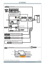
Use of committed pilot wire output BLOUT1:
The information about phase or phase+earth block may be select programming the
ModeBLOUT1
parameter inside
Set \ Profi le A(or B) \ Selective block-BLOCK2 \ Selective block OUT
menus.
Use of output relay (K1...K6):
If the
DthAL1BLK2OUT, DthAL2BLK2OUT
and/o
Dth>BLK2OUT
enable parameters are set
to
ON
and a output relay is designed for selective block (Block2), the protection issues a block
output by phase elements (BLK2OUT-Iph) or by any protection element (BLK2OUT-Iph/IE), when-
ever the given element (DthAL1, DthAL2 e/o Dth>) becomes active. The enable
DthAL1BLK2OUT,
DthAL2BLK2OUT
and/or
Dth>BLK2OUT
parameters are available inside the
Set \ Profi le
A(or B) \Thermal image-49 \
DthAL1 Element
(
DthAL2 Element
,
Dth> Element)
menus, while the
BLK2OUT-Iph-K, BLK2OUT-Iph/IE-K
and/or
BLK2OUT-IE-K
output relays must be set in-
side the
Set \ Profi le A(or B) \ Selective block-BLOCK2 \ Selective block OUT
menus.
Note 1 The exhaustive treatment of the logical block (Block 1) function may be found in the “Logic Block” paragraph inside
CONTROL AND MONITOR-
ING
section
Note 2 The exhaustive treatment of the selective block (Block 2) function may be found in the “Selective Block” paragraph inside
CONTROL AND
MONITORING
section
•
•
•
•
•
•
•
•