1-3-1
T6600STA
STANDARD NOTES FOR SERVICING
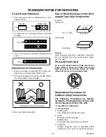
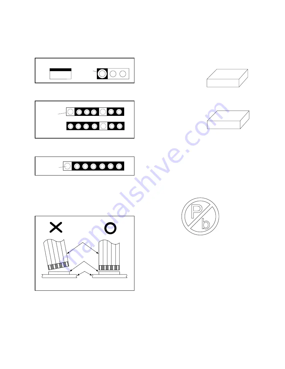
Circuit Board Indications
1. The output pin of the 3 pin Regulator ICs is indi-
cated as shown:
2. For other ICs, pin 1 and every 5th pin is indicated
as shown:
3. The 1st pin of every pin connector are indicated as
shown:
Instructions for Connectors
1. When you connect or disconnect FFC cable (con-
nector), be sure to disconnect the AC cord.
2. FFC cable (connector) should be inserted parallel
into the connector, not at an angle.
[ CBA= Circuit Board Assembly ]
How to Read the Values of the Rect-
angular Type Chip Components
Example:
(a) Resistor
(b) Capacitor
Caution:
Once chip parts (Resistors, Capacitors, Transistors,
etc.) are removed, they must not be reused. Always
use a new part.
Pb (Lead) Free Solder
Pb free mark will be found on PCBs used Pb free
solder. (Refer to figure.) For PCBs with Pb free
mark, be sure to use Pb free solder. For PCBs
without Pb free mark, use standard solder.
Replacement Procedures for
Leadless (Chip) Components
The Following Procedures are Recom-
mended for the Replacement of the Lead-
less Components Used in this Unit.
1. Preparation for replacement
1.1. Pb free solder
a. Soldering Iron
Use a soldering iron for Pb free solder.
b. Solder
Be sure to use Pb free solder.
c. Soldering time
Do not apply heat for more than 4 seconds.
d. Preheating
Leadless capacitor must be preheated before
installation. (130°C~150°C, for about two minutes.)
Top View
Out
In
Bottom View
Input
5
10
Pin 1
Pin 1
FFC Cable
Connector
CBA
* Be careful to avoid a short circuit.
(Top View)
473
= 473 = 47 [k
Ω
]
(Top View)
= Not Shown
Pb free mark
Summary of Contents for LT-VHS-36
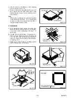
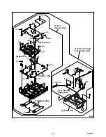
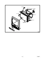
Page 17: ...1 5 4 T6608DC Fig 4 S 10 S 10 S 10 S 10 Anode Cap 11 CRT CRT CBA...
Page 36: ...Main 1 5 Schematic Diagram 1 8 3 1 8 4 T6608SCM1...
Page 37: ...Main 2 5 Schematic Diagram 1 8 5 1 8 6 T6608SCM2...
Page 38: ...Main 3 5 Schematic Diagram 1 8 7 1 8 8 T6608SCM3...
Page 39: ...Main 4 5 Schematic Diagram 1 8 9 1 8 10 T6608SCM4...
Page 40: ...1 8 11 1 8 12 T6608SCM5 Main 5 5 Schematic Diagram...
Page 42: ...1 8 15 1 8 16 H V Power Supply 2 2 Schematic Diagram T6608SCP2...
Page 43: ...1 8 17 1 8 18 T6608SCCRT CRT Schematic Diagram...
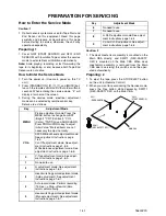
Page 58: ...1 14 3 T6608PEX Packing S3 S6 X3 S2 X1 TAPE S1 FRONT S4 X2 1 X2 2 X2 6...
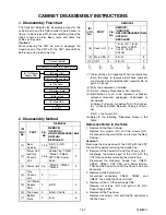
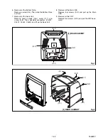
Page 91: ...2 4 9 Z13PDA Fig DM16 43 41 42 L 13 Fig DM17 44 45 Slide P 9...
Page 98: ...LT VHS 36 T6608FJ 2004 06 03...


