background image

A

B

C

D

E

F

G

H

A

B

C

D

E

F

G

H

2

1

3

4

5

6

7

8

2

1

3

4

5

6

7

8

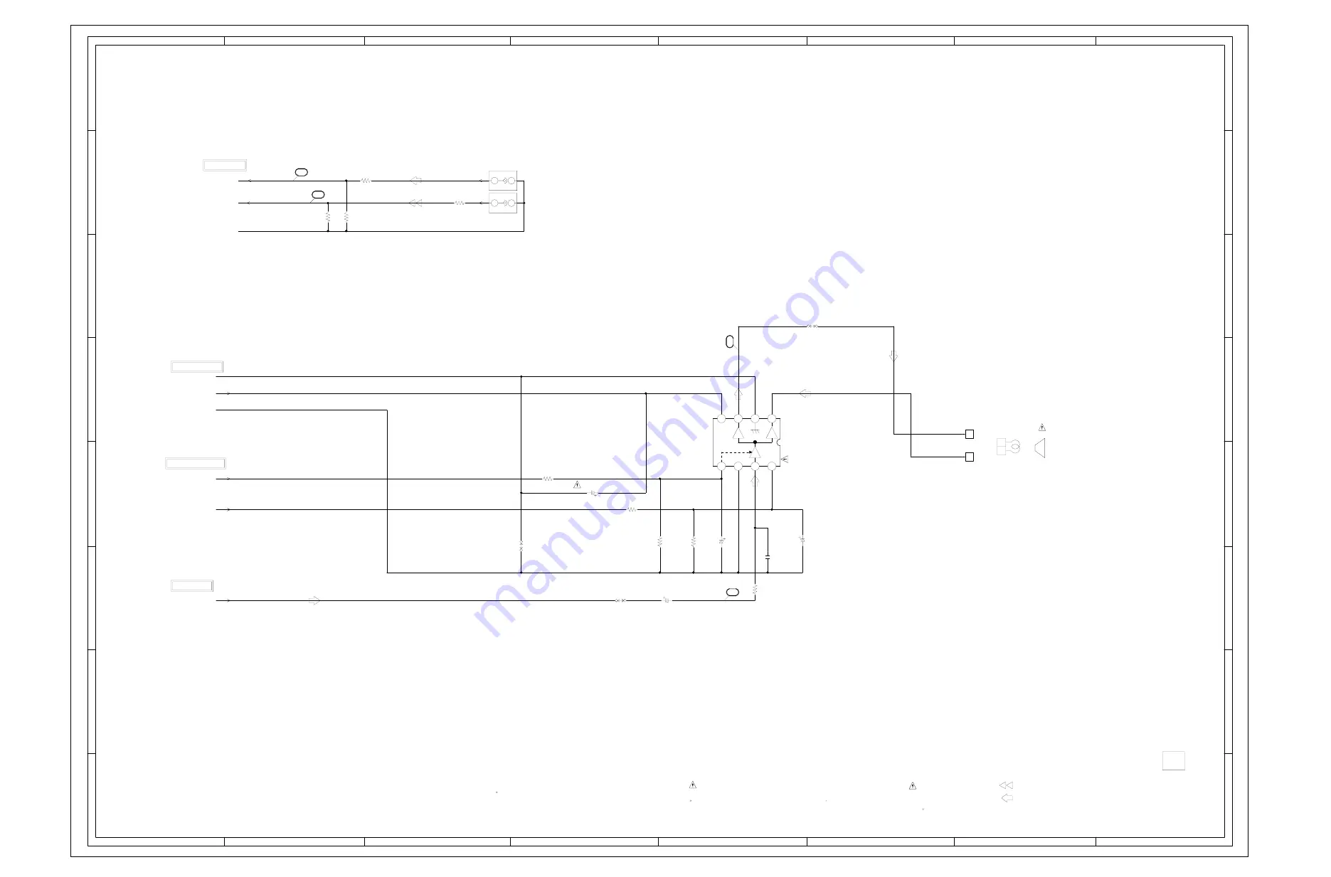
SPEAKER

SP1001
S08F21

8 OHM

CD101A

CH012002

1

CD101B

CH012003

1

H

E

J703

AV1-09D-4

1

2

H

E

J702

AV1-09D-3

1

2

AUDIO SIGNAL

THE DC VOLTAGE AT EACH PART WAS MEASURED

 WITH THE DIGITAL TESTER WHEN THE COLOR BROADCAST

WAS RECEIVED IN GOOD CONDITION AND PICTURE IS NORMAL.

NOTE:

C1004_1

0.0015

CH

C1001

0.1

50V

KA

C1005

10

25V

KA

R703

820

R1003

68K

R1005

270K

R1004

100K

R1001

47K

R1008

68K

R702

47K

R701

68

1/4W

R704

10

OF PRINTING AND SUBJECT TO CHANGE WITHOUT NOTICE

NOTE: THIS SCHEMATIC DIAGRAM IS THE LATEST AT THE TIME

DANS LA NOMENCLATURE DES PIECES

N’UTILISER QUE CELLS DECRITES

DANGEREUSES AN POINT DE VUE SECURITE

ETANT

LES PIECES REPAREES PAR UN

ATTENTION:

DESCRIBED IN PARTS LIST ONLY

CRITICAL FOR SAFETY,USE ONES

ARE

SINCE THESE PARTS MARKED BY

CAUTION:

W807

W803

W805

C1002_1

470

10V

YK

C1003

1

50V

KA

IC1001

AN7511

SOUND AMP IC

1

2

3

4

5

6

7

8

TUNER VIDEO SIGNAL

AUDIO_IN

VIDEO_IN

GND

SOUND_GND

SOUND+B

GND

AUDIO_MUTE

POWER

AUDIO_OUT

TO CHROMA

1

2

FROM CHROMA

FROM MICON/TUNER

-

+

0

0

8.2

3.5

3.4

3.9

5.1

0.3

FROM TV POWER

24

23

VIDEO 2

AUDIO 2

26

25

(FRONT)

V_IN

A_IN

PCB010

SOUND/AV SCHEMATIC DIAGRAM

(MAIN PCB)

TMB535

Summary of Contents for 20AS22

Page 1: ...SERVICE MANUAL COLOR TELEVISION FILE NO 050 200206 20AS22 DOCUMENT CREATED IN JAPAN May 2002 ...

Page 2: ...t which has the same character Especially as to the important parts for safety which is indicated in the circuit diagram or the table of parts as a mark the designated parts must be used 4 PUT PARTS AND WIRES IN THE ORIGINAL POSITION AFTER ASSEMBLING OR WIRING There are parts which use the insulation material such as a tube or tape for safety or which are assembled in the condition that these do n...

Page 3: ...ve CH Destination Ohers Tuning System F Synth Input Impedance VHF UHF 75 ohm 2 69 4A A 5 A 1 CH Coverage A I J W W 1 W 84 Intermediate Picture FP 45 75MHz Frequency Sound FS 41 25MHz FP FS 4 50MHz Preset CH No Stereo Dual TV Sound No Tuner Sound Muting Yes G 3 Power Power Source AC 120V AC 60Hz DC Power Consumption at AC 73 W at AC 120 V 60 Hz Stand by at AC 5 W at AC 120 V 60 Hz Per Year kWh Year...

Page 4: ...Stream DVD DTV No Control Level Yes Volume Yes Brightness Yes Contrast Yes Color Yes Tint NTSC Only Yes Sharpness Yes Tuning No Bass No Treble No Balance No Back Light No Stereo Audio Output SAP No Video Yes Color Stream No Channel TV Cable Yes CH Label No Game Timer Yes Sleep Timer Yes Sound Mute Yes V chip Rating Yes G 8 OSD Language English French Spanish OSD Language Setting English G 9 Clock ...

Page 5: ...es 5 Yes 6 Yes 7 Yes 8 Yes 9 Yes 0 Yes 100 No CH Up Yes CH Down Yes Volume Up Yes Volume Down Yes TV Caption Text Yes CH1 CH2 Yes TV Video TV AV Yes CH RTN CH ENT Quick View Yes Sleep Yes RE Call Call Yes Reset Yes Menu Yes Enter Yes Mute Yes Exit No MTS Audio Select No Set Yes Set Yes Multi Brand Keys CH Up VCR No CH Down VCR No Pause Still No TV VCR VCR No Code No FF No Rew No Rec No Play No Sto...

Page 6: ...ock Yes Video Lock Yes Game Timer Yes Energy Star No Favorite CH No G 12 Accessories Owner s Manual Language English Spanish W Warranty Yes Remote Control Unit Yes Rod Antenna No Poles Terminal Loop Antenna No Terminal U V Mixer No DC Car Cord Center No Guarantee Card No Warning Sheet No Circuit Diagram No Antenna Change Plug No Service Facility List No Important Safety Instruction Yes Dew AHC Cau...

Page 7: ...r2 No Video Output No Audio Output No Euro Scart No Color Stream No Diversity No Ext Speaker No DC Jack 12V Center No VHF UHF Antenna Input F Type AC Outlet No G 14 Set Size Approx W x D x H mm 488 x 465 x 416 G 15 Weight Net Approx 17 5kg 38 6 lbs Gross Approx 20 0kg 44 1lbs G 16 Carton Master Carton No Content Sets Material Dimensions W x D x H mm x x Description of Origin No Gift Box Yes Materi...

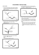
Page 8: ... Flip up the sides of the Rubber Cap in the direction of the arrow and remove one side of the support Refer to Fig 1 2 2 DISASSEMBLY INSTRUCTIONS GND on the CRT Screwdriver Alligator Clip Support CRT GND on the CRT Rubber Cap CRT Support Fig 1 1 Fig 1 2 3 After one side is removed pull in the opposite direction to remove the other NOTE Take care not to damage the Rubber Cap INSTALLATION 1 Clean th...

Page 9: ...ng a blower type IC desoldering machine Refer to Fig 2 2 2 Fig 2 2 NOTE Do not add the rotating and the back and forth directions force on the IC until IC can move back and forth easily after desoldering the IC leads completely When IC starts moving back and forth easily after desoldering completely pickup the corner of the IC using a tweezers and remove the IC by moving with the IC desoldering ma...

Page 10: ... Thin tip Soldering Iron NOTE When the IC leads are bent during soldering and or repairing do not repair the bending of leads If the bending of leads are repaired the pattern may be damaged So be always sure to replace the IC in this case Finally confirm the soldering status on four sides of the IC using a magnifying glass Confirm that no abnormality is found on the soldering position and installa...

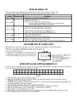
Page 11: ...re than 1 second After the confirmation of using hours turn off the power WHEN REPLACING EEPROM MEMORY IC If a service repair is undertaken where it has been required to change the MEMORY IC the following steps should be taken to ensure correct data settings while making reference to TABLE 1 Table 1 1 2 3 4 5 6 7 8 The unit will now have the correct DATA for the new MEMORY IC Enter DATA SET mode b...

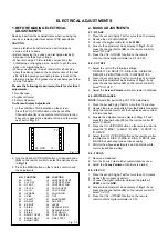
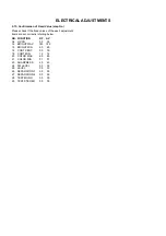
Page 12: ...the screen as shown in Fig 1 1 1 Fig 1 1 Use the Channel UP DOWN button or Channel button 0 9 on the remote control to select the options shown in Fig 1 2 Press the MENU button on the remote control to end the adjustments 2 3 Prepare the following measurement tools for electrical adjustments FUNCTION OSD H CUT OFF RF AGC VIF VCO H VCO H PHASE V SIZE V SHIFT R DRIVE B DRIVE R BIAS G BIAS B BIAS BRI...

Page 13: ... control set the brightness and contrast to normal position Activate the adjustment mode display of Fig 1 1 and press the channel button 07 on the remote control to select V SFT Press the VOL UP DOWN button on the remote control until the horizontal line becomes fit to the notch of the shadow mask 2 11 SUB TINT SUB COLOR 1 2 3 4 5 6 7 8 9 10 Receive the color bar pattern RF Input Connect the oscil...

Page 14: ...3 Confirmation of Fixed Value step No NO 04 14 15 16 18 20 21 23 24 25 26 27 28 29 FUNCTION H VCO BRIGHT MAX BRIGHT MIN CONT CENT CONT MIN COLOR MAX COLOR MIN SHARPNESS FM LEVEL LEVEL SEPARATION 1 SEPARATION 2 TEST MONO TEST STEREO RF 05 183 60 30 12 65 01 40 00 00 00 00 00 00 AV 05 183 60 30 12 65 01 40 00 00 00 00 00 00 ...

Page 15: ...rforming adjustments in section 3 1 1 2 3 4 5 Receive the green raster pattern from color bar generator Adjust the pair of purity magnets to center the color on the screen Adjust the pair of purity magnets so the color at the ends are equally wide Move the deflection yoke backward to neck side slowly and stop it at the position when the whole screen is green Confirm red and blue color Adjust the s...

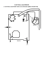
Page 16: ...4 ELECTRICAL ADJUSTMENT PARTS LOCATION GUIDE WIRING CONNECTION TU001 FB401 S501B S501A AC IN CP601 CP502 CD101B CD101A W043 CP401 SPEAKER R807 R803 J801 CP806 L503 CRT CRT PCB CRT C P 8 0 2 A CRT C D 8 0 1 C P 8 0 1 CP802B TP023 TP022 ...

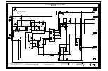
Page 17: ... AUDIO OUT 8 7V REG OUT R OUT G OUT B OUT POWER ON CONT H OUT X TAL RF AGC OUT VIF IN 1 VIF IN 2 V PULSE OUT SCL SDA MCU RESET V OUT KEY2 7 SDA SCL 19 INV FBP OUT 38 H SYNC 24 33 BLANK FAST BLK 21 B IN 36 BLUE B 22 35 GREEN G G IN 23 R IN 34 RED R 26 CVIN 31 Y SW OUT 32 AT5 7V REG OUT 42 VREG VCC 10 FBP IN Q603 REG DY 49 P CON 5 7V REG Q604 Q605 REG D501 D504 RECTIFIER 3 1 4 2 L501 AC IN F501 R SI...

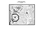
Page 18: ..._1 C612 D610 D611 D612 W022 R614 C603 Q610 W817 Q609_1 R627 R631 R630 R629 W023 W024 R606 D605 W027 C519 W030 R805 W031 CP802B Q803 Q801 Q802 R806 R803 R807 J 8 0 1 C118 W034 R401 R408 D619 W036 D406_1 Q506 W804 R514 W040 W041 CF601_1 W042 W043 W044 C647 W806 W821 W829 W844 C645 R804_1 R802_1 R512 W046 W047 R641 R525 R519 R518 D514 R513 R110 W049 CD101B CD101A C801 W050 D403 D405 D411 W051 C119 W8...

Page 19: ...102 R123 R103 R121 R120 R106 R105 R130 C121 C138 R134 R601 R602 R609 R622 R615 C655 R639 R632 R633 R646 R642 C140_2 R619 R625 R605 R617 R141 R142 R811 R809 R814 R815 R813 R816 R129 R638 R626 R1001 R133 R612 R111 C810 C808 C809 R118 R1008 R125 C618_1 C623 R607 R628 R116 PRINTED CIRCUIT BOARDS MAIN CRT CHIP MOUNTED PARTS SOLDER SIDE ...

Page 20: ...3uH SW101 SKHVBED010 CH UP SW102 SKHVBED010 CH DOWN SW103 SKHVBED010 VOL UP SW104 SKHVBED010 VOL DOWN SW105 SKHVBED010 POWER TU001 ENV56DB6G3 1 10 11 12 13 14 15 2 3 4 5 6 7 8 9 C118 330 6 3V YK C128_1 330 6 3V YK IC199 S 24C02BDP 1A MEMORY IC 1 2 3 4 5 6 7 8 GND B Vout OS101 PIC 37143SY 1 2 3 IC101 OEC7072A MICON IC 1 10 11 12 13 14 15 16 17 18 19 2 20 21 22 23 24 25 26 27 28 29 3 30 31 32 33 34 ...

Page 21: ... DECRITES DANGEREUSES AN POINT DE VUE SECURITE ETANT LES PIECES REPAREES PAR UN ATTENTION DESCRIBED IN PARTS LIST ONLY CRITICAL FOR SAFETY USE ONES ARE SINCE THESE PARTS MARKED BY CAUTION D612 MTZJ12B D610 MTZJ12B D602 MTZJ8 2B D606 MTZJ6 8B T 77 D611 MTZJ12B W833 W842 W823 W818 W820 W817 W834 L607 15uH DEFLECTION SIGNAL B SIGNAL G SIGNAL R SIGNAL TUNER VIDEO SIGNAL UNREG 12V VIDEO_IN AUDIO_OUT RE...

Page 22: ...C VOLTAGE AT EACH PART WAS MEASURED WITH THE DIGITAL TESTER WHEN THE COLOR BROADCAST WAS RECEIVED IN GOOD CONDITION AND PICTURE IS NORMAL NOTE C522 0 001 B C513_1 0 082 MMT C518 470P 500V B C505 0 22 275V PHE840 C502 0 001 500V B C503 0 001 500V B C506 0 0047 250V KX C509 0 047 M C517 470P 2KV RR C501 0 0082 M C514 680P 2KV RR C516 0 001 2KV RR C511 1 50V KA C526 330 200V UP C530 10 100V MHE R509_...

Page 23: ...100K 1 4W R445 150K 1 4W R427 100 1 4W R416 1 1 2W R815 330 R813 330 R420 4 7K R806 2 7K 1 4W R410 330 1 2W R415 1 8K 1 2W R816 330 R413 2 2K 1 2W R403 22K 1 4W R422 1 8 1 2W R419 560 R417 12K 1 4W R446 470 1 2W R423 100 1 4W R424 6 8K R802_1 2 7K 1 4W R804_1 2 7K 1 4W R402 27 1 2W R814 4 7K R811 4 7K R809 4 7K OF PRINTING AND SUBJECT TO CHANGE WITHOUT NOTICE NOTE THIS SCHEMATIC DIAGRAM IS THE LAT...

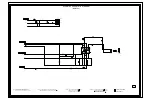
Page 24: ...AND SUBJECT TO CHANGE WITHOUT NOTICE NOTE THIS SCHEMATIC DIAGRAM IS THE LATEST AT THE TIME DANS LA NOMENCLATURE DES PIECES N UTILISER QUE CELLS DECRITES DANGEREUSES AN POINT DE VUE SECURITE ETANT LES PIECES REPAREES PAR UN ATTENTION DESCRIBED IN PARTS LIST ONLY CRITICAL FOR SAFETY USE ONES ARE SINCE THESE PARTS MARKED BY CAUTION W807 W803 W805 C1002_1 470 10V YK C1003 1 50V KA IC1001 AN7511 SOUND ...

Page 25: ...iv 200mV 20µs div 7 9 200mV 20µs div CHROMA 0 5V 5ms div 10 11 1V 20µs div 12 1V 20µs div 1V 20µs div 13 8 20V 20µs div 3 200mV 20µs div DEFLECTION CRT 14 0 5V 5ms div 15 20V 20µs div NOTE The following waveforms were measured at the point of the corresponding balloon number in the schematic diagram ...

Page 26: ...20µs div SOUND AV 0 5V 1ms div 23 10V 5ms div 18 10V 5ms div 19 1V 1ms div 24 50V 20µs div 20 NOTE The following waveforms were measured at the point of the corresponding balloon number in the schematic diagram WAVEFORMS 200mV 500µs div 25 26 500mV 20µs div ...

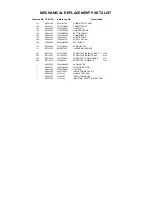
Page 27: ...MECHANICAL EXPLODED VIEW 201 201 201 110 201 PCB110 CRT PCB 204 PCB010 MAIN PCB 203 204 111 101 102 104 103 105 108 106 107 202 202 202 202 109 109 ...

Page 28: ...ON 109 AD300844 800WQ00038 FELT SHEET 110 BZ710009 741WUA0019 SPRING EARTH 111 BZ710260 899HV3T000 HOLDER ANODE WIRE 201 BZ710321 8121F50B84 SCREW TAPPING B0 FAI20 FLAT 5x28 202 BZ710035 8117540A64 SCREW TAPPING B0 TRUSS 4x16 203 BZ710018 8107630804 SCREW TAP TITE S BRAZIER 3x8 204 BZ710239 8109I30A04 SCREW TAP TITE B WH7 3x10 AD300700 792WHAA054 PACKAGE TOP AD300701 792WHAA055 PACKAGE BOTTOM AD30...

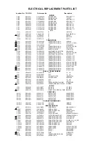
Page 29: ...514 AD301320 C0PLRR7U2K CC 680 PF 2KV RR C515 AD300925 E02LT2102M CE 1000 UF 16V C516 BZ110202 C0PLRR713K CC 0 001 UF 2KV RR C517 BZ110219 C0PLRR7Q2K CC 470 PF 2KV RR C519 BZ110081 E02LT2471M CE 470 UF 16V C521 BZ110092 E5EZFB101M CE 100 UF 160V C522 BZ110173 CHG0B0413K CC 0 001 UF 50V B or AD301466 CHG0B0413J CC 0 001 UF 50V B or BZ110098 CHGTB0413K CC 0 001 UF 50V B or AD301467 CHGTB0413J CC 0 0...

Page 30: ...10091 TCA0042170 TRANSISTOR SILICON KTC4217 O Y COILS TRANSFORMERS L101 AD300676 021LA63R3K COIL 3 3 UH L402 AD301394 02186G180M COIL 18 UH L501 AD301395 029T000104 COIL LINE FILTER 1R0A562F20 L503 BZ310092 028R200029 COIL DEGAUSS 8R200029 L607 BZ310043 021LA6150K COIL 15 UH L801 BZ310005 02167D101K COIL 100 UH T401 BZ310157 045009003J TRANS HORIZONTAL DRIVE ETH09K14BZ T502 AD301396 048129092S TRA...

Page 31: ...TH501 BZ410056 DF20A3R0Q0 DEGAUSS ELEMENT PTDAA1BF3R0Q100 TM101 AD301335 076N0EH020 TRANSMITTER RC EH020 TU001 AD301052 0145100059 TUNER VHF UHF ENV56DB6G3 V801 AD301399 098Y200484 CRT W DY A48LGS30X19N35 X602 BZ613004 100CT3R505 CRYSTAL HC 49 C RESISTOR RC CARBON RESISTOR CAPACITORS CC CERAMIC CAPACITOR CE ALUMI ELECTROLYTIC CAPACITOR CP POLYESTER CAPACITOR CPP POLYPROPYLENE CAPACITOR CPL PLASTIC...

Page 32: ...TOSHIBA CORPORATION 1 1 SHIBAURA 1 CHOME MINATO KU TOKYO 105 8001 JAPAN ...

Reviews: