background image

ELECTRICAL ADJUSTMENTS

D-5

27A45/27A45C

3-3: STATIC CONVERGENCE

NOTE

Adjust after performing adjustments in section 3-2.

1.

2.

3.

Receive the crosshatch pattern from the color bar
generator.
Combine red and blue of the 3 color crosshatch
pattern on the center of the screen by adjusting the pair
of 4 pole magnets.
Combine red/blue (magenta) and green by adjusting the
pair of 6 pole magnets.

3-4: DYNAMIC CONVERGENCE

NOTE

Adjust after performing adjustments in section 3-3.

1.

2.

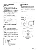
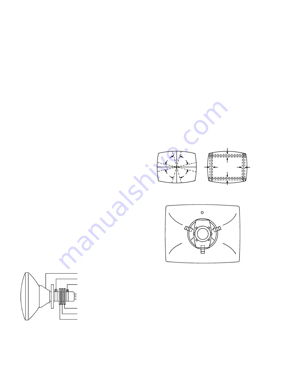
Adjust the differences around the screen by moving the
deflection yoke upward/downward and right/left.
(Refer to Fig. 3-2-a)
Insert three wedges between the deflection yoke and
CRT funnel to fix the deflection yoke.
(Refer to Fig. 3-2-b)

R G B

R
G
B

R
G
B

R G B

UPWARD/DOWNWARD SLANT    RIGHT/LEFT SLANT

Fig. 3-2-a

WEDGE

WEDGE

WEDGE

WEDGE POSITION

Fig. 3-2-b

DEFLECTION YOKE SCREW

3. PURITY AND CONVERGENCE

ADJUSTMENTS

NOTE

1.

2.

3.

Turn the unit on and let it warm up for at least 30
minutes before performing the following adjustments.
Place the CRT surface facing east or west to reduce the
terrestrial magnetism.
Turn ON the unit and demagnetize with a Degauss Coil.

3-1: STATIC CONVERGENCE (ROUGH ADJUSTMENT)

1.

2.

3.

4.

5.

6.

7.

8.

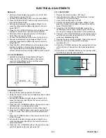
Tighten the screw for the magnet. Refer to the adjusted
CRT for the position. (Refer to Fig. 3-1)
If the deflection yoke and magnet are in one body,
untighten the screw for the body.
Receive the green raster pattern from the color bar
generator.
Slide the deflection yoke until it touches the funnel side
of the CRT.
Adjust center of screen to green, with red and blue on
the sides, using the pair of purity magnets.
Switch the color bar generator from the green raster
pattern to the crosshatch pattern.
Combine red and blue of the 3 color crosshatch
pattern on the center of the screen by adjusting the pair
of 4 pole magnets.
Combine red/blue (magenta) and green by adjusting the
pair of 6 pole magnets.
Adjust the crosshatch pattern to change to white by
repeating steps 6 and 7.

3-2: PURITY

NOTE

Adjust after performing adjustments in section 3-1.

1.
2.

3.

4.
5.

Receive the green raster pattern from color bar genera-
tor.
Adjust the pair of purity magnets to center the color on
the screen.
Adjust the pair of purity magnets so the color at the ends
are equally wide.
Move the deflection yoke backward (to neck side)
slowly, and stop it at the position when the whole screen
is green.
Confirm red and blue color.
Adjust the slant of the deflection yoke while watching the
screen, then tighten the fixing screw.

DEFLECTION YOKE

MAGNET SCREW

PURITY MAGNETS
6 POLE MAGNETS
4 POLE MAGNETS

Fig. 3-1

Summary of Contents for 27A45

Page 1: ...SERVICE MANUAL COLOR TELEVISION DOCUMENT CREATED IN JAPAN February 2005 27A45 FILE NO 050 200505 27A45C MFR S VERSION A ...

Page 2: ...be used the part which has the same character Especially as to the important parts for safety which is indicated in the circuit diagram or the table of parts as a mark the designated parts must be used 4 PUT PARTS AND WIRES IN THE ORIGINAL POSITION AFTER ASSEMBLING OR WIRING There are parts which use the insulation material such as a tube or tape for safety or which are assembled in the condition ...

Page 3: ...dering iron please be carefull not to heat too long Pb free solder will tend to splash when heated too high about 1100 F 600 C All products with the printed circuit board with PbF printing must be serviced with lead free solder When soldering or unsoldering completely remove all of the solder from the pins or solder area and be sure to heat the soldering points with the lead free solder until it m...

Page 4: ...EPROM MEMORY IC ELECTRICAL ADJUSTMENTS BLOCK DIAGRAMS PRINTED CIRCUIT BOARDS MAIN CRT SCHEMATIC DIAGRAMS MICON CHROMA DEFLECTION POWER SOUND TUNER STEREO AV CRT COMB FILTER WAVEFORMS MECHANICAL EXPLODED VIEWS MECHANICAL REPLACEMENT PARTS LIST ELECTRICAL REPLACEMENT PARTS LIST A1 1 A1 1 A1 1 A1 2 A2 1 A3 1 A3 10 B1 1 B2 1 B2 2 C1 1 C1 1 C1 1 D 1 D 6 E 1 E 2 F 1 F 4 G 1 G 2 G 3 G 4 G 5 G 6 G 7 G 8 G...

Page 5: ...tion USA W CATV 2 69 4A A 5 A 1 CH Coverage A I J W W 1 W 84 Intermediate Picture FP 45 75MHz Frequency Sound FS 41 25MHz FP FS 4 50MHz Preset CH No Stereo Dual TV Sound Yes Tuner Sound Muting Yes G 3 Power Power Source AC 120V AC 60Hz DC Power Consumption at AC 125 W at AC 120 V 60 Hz Stand by at AC 3 W at AC 120 V 60 Hz Per Year kWh Year Protector Power Fuse Yes Safety Circuit Yes IC Protector M...

Page 6: ...n Off Timer Yes Color Stream DVD DTV Yes Control Level Yes Volume Yes Brightness Yes Contrast Yes Color Yes Tint Yes Sharpness Yes Tuning No Bass Yes Treble Yes Balance Yes Back Light No Stereo Audio Output SAP Yes Video Yes Color Stream Yes Channel TV Cable Yes CH Label Yes Game Timer Yes Sleep Timer Yes Sound Mute Yes V chip Rating Yes 16 9 No G 8 OSD Language English French Spanish G 9 Clock an...

Page 7: ... CH Down Yes Volume Up Yes Volume Down Yes TV Caption Text Yes CH1 CH2 Yes TV Video TV AV Yes CH RTN CH ENT Quick View Yes Sleep Yes RE Call Call Yes Reset Yes Menu Enter Yes Mute Yes Exit Yes MTS Audio Select Yes Fav Up Yes Fav Down Yes 16 9 No Multi Brand Keys CH Up VCR Yes CH Down VCR Yes Pause Still Yes TV VCR VCR Yes FF Yes Rew Yes Rec Yes Play Yes Stop Yes TV Yes VCR Yes Cable Yes DVD Yes CO...

Page 8: ...Max Time 120 Min Yes Energy Star No Favorite CH Yes Surround Yes 16 9 Mode No 2 Tuner P in P No G 12 Accessories Owner s Manual Language English Spanish W Warranty Yes Remote Control Unit Yes Rod Antenna No Poles Terminal Loop Antenna No Terminal U V Mixer No DC Car Cord Center No Guarantee Card No Warning Sheet No Circuit Diagram No Antenna Change Plug No Service Facility List No Important Safety...

Page 9: ...t Speaker No DC Jack 12V Center No VHF UHF Antenna Input F Type AC Outlet No G 14 Set Size Approx W x D x H mm 740 x 491 5 x 571 5 G 15 Weight Net Approx 37 0kg 81 6 lbs Gross Approx 41 0Kg 90 4 lbs G 16 Carton Master Carton No Content Sets Material Dimensions W x D x H mm x x Description of Origin No Gift Box Material Double Brown Dimensions W x D x H mm 850 x 575 x 665 Design As per Buyer s Desc...

Page 10: ...tion USA W CATV 2 69 4A A 5 A 1 CH Coverage A I J W W 1 W 84 Intermediate Picture FP 45 75MHz Frequency Sound FS 41 25MHz FP FS 4 50MHz Preset CH No Stereo Dual TV Sound Yes Tuner Sound Muting Yes G 3 Power Power Source AC 120V AC 60Hz DC Power Consumption at AC 125 W at AC 120 V 60 Hz Stand by at AC 3 W at AC 120 V 60 Hz Per Year kWh Year Protector Power Fuse Yes Safety Circuit Yes IC Protector M...

Page 11: ... Off Timer Yes Color Stream DVD DTV Yes Control Level Yes Volume Yes Brightness Yes Contrast Yes Color Yes Tint Yes Sharpness Yes Tuning No Bass Yes Treble Yes Balance Yes Back Light No Stereo Audio Output SAP Yes Video Yes Color Stream Yes Channel TV Cable Yes CH Label Yes Game Timer Yes Sleep Timer Yes Sound Mute Yes V chip Rating No 16 9 No G 8 OSD Language English French Spanish G 9 Clock and ...

Page 12: ... CH Down Yes Volume Up Yes Volume Down Yes TV Caption Text Yes CH1 CH2 Yes TV Video TV AV Yes CH RTN CH ENT Quick View Yes Sleep Yes RE Call Call Yes Reset Yes Menu Enter Yes Mute Yes Exit Yes MTS Audio Select Yes Fav Up Yes Fav Down Yes 16 9 No Multi Brand Keys CH Up VCR Yes CH Down VCR Yes Pause Still Yes TV VCR VCR Yes FF Yes Rew Yes Rec Yes Play Yes Stop Yes TV Yes VCR Yes Cable Yes DVD Yes CO...

Page 13: ...me 120 Min Yes Energy Star No Favorite CH Yes Surround Yes 16 9 Mode No 2 Tuner P in P No G 12 Accessories Owner s Manual Language English French W Warranty Yes Remote Control Unit Yes Rod Antenna No Poles Terminal Loop Antenna No Terminal U V Mixer No DC Car Cord Center No Guarantee Card No Warning Sheet No Circuit Diagram No Antenna Change Plug No Service Facility List No Important Safety Instru...

Page 14: ... Speaker No DC Jack 12V Center No VHF UHF Antenna Input F Type AC Outlet No G 14 Set Size Approx W x D x H mm 740 x 491 5 x 571 5 G 15 Weight Net Approx 37 0kg 81 6 lbs Gross Approx 41 0Kg 90 4 lbs G 16 Carton Master Carton No Content Sets Material Dimensions W x D x H mm x x Description of Origin No Gift Box Material Double Brown Dimensions W x D x H mm 850 x 575 x 665 Design As per Buyer s Descr...

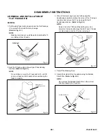
Page 15: ...ischarged Flip up the sides of the Rubber Cap in the direction of the arrow and remove one side of the support Refer to Fig 1 2 2 DISASSEMBLY INSTRUCTIONS GND on the CRT Screwdriver Alligator Clip Support CRT GND on the CRT Rubber Cap CRT Support Fig 1 1 Fig 1 2 3 After one side is removed pull in the opposite direction to remove the other NOTE Take care not to damage the Rubber Cap INSTALLATION 1...

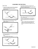
Page 16: ...IC Heat the IC leads using a blower type IC desoldering machine Refer to Fig 2 2 2 Fig 2 2 NOTE Do not rotate or move the IC back and forth until IC can move back and forth easily after desoldering the leads completely When IC starts moving back and forth easily after desoldering completely pickup the corner of the IC using a tweezers and remove the IC by moving with the IC desoldering machine Ref...

Page 17: ...4 Fig 2 8 Thin tip Soldering Iron NOTE When the IC leads are bent during soldering and or repairing do not repair the bending of leads If the bending of leads are repaired the pattern may be damaged So always be sure to replace the IC in this case Finally confirm the soldering status on four sides of the IC using a magnifying glass Confirm that no abnormality is found on the soldering position and...

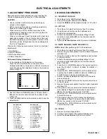
Page 18: ...igit value C 1 WHEN REPLACING EEPROM MEMORY IC If a service repair is undertaken where it has been required to change the MEMORY IC the following steps should be taken to ensure correct data settings while making reference to TABLE 1 Table 1 1 2 3 4 5 6 7 8 9 10 11 The unit will now have the correct DATA for the new MEMORY IC Enter DATA SET mode by setting VOLUME to minimum Press both VOL DOWN but...

Page 19: ...32 33 34 35 88 2 BASIC ADJUSTMENTS 2 1 CONSTANT VOLTAGE 1 2 3 Place the set in AV MODE without signal Connect the digital voltmeter to the TP003 Adjust the VR502 until the digital voltmeter is 123 0 5V 2 2 CUT OFF 1 2 3 4 Place the set in Aging Test for more than 15 minutes Using the remote control set the brightness and contrast to normal position Activate the adjustment mode display of Fig 1 1 a...

Page 20: ...downside becomes minimum 1 2 3 4 2 9 TRAPEZIUM 1 2 3 4 Receive the cross hatch signal from the Pattern Generator Using the remote control set the brightness and contrast to normal position Activate the adjustment mode display of Fig 1 1 and press the channel button 32 on the remote control to select TRAPEZIUM Press the VOL UP DOWN button on the remote control until the both vertical lines of the s...

Page 21: ...remote control until the red color level is adjusted to 120 10 of the white level Refer to Fig 2 3 Receive the video color bar pattern Audio Video Input Set to the AV mode Then perform the above adjustments 2 6 Press the TV VIDEO button on the remote control to set to the CS mode Then perform the above adjustments 2 4 Press the VOL UP DOWN button on the remote control until the color step No becom...

Page 22: ...ode display of Fig 1 1 and press the channel button 18 on the remote control to select CONT MAX Press the VOL UP DOWN button on the remote control until the contrast step No becomes 85 Receive a broadcast and check if the picture is normal Press the TV VIDEO button on the remote control to set to the AV mode Then perform the above adjustments 1 3 Press the TV VIDEO button on the remote control to ...

Page 23: ...6 7 8 Tighten the screw for the magnet Refer to the adjusted CRT for the position Refer to Fig 3 1 If the deflection yoke and magnet are in one body untighten the screw for the body Receive the green raster pattern from the color bar generator Slide the deflection yoke until it touches the funnel side of the CRT Adjust center of screen to green with red and blue on the sides using the pair of puri...

Page 24: ... PARTS LOCATION GUIDE WIRING CONNECTION CP803 CP801B CP802B CD802 CP806 J801 W003 TP003 VR502 CP101 CP801A FB401 CP802A TU001 VR401 CD801 CP401 CP1001 CRT PCB MAIN PCB R803 R805 TP024 TP022 SPEAKER CRT CP502 CRT L503 CP501 CD501 AC IN CRT 27A45 27A45C ...

Page 25: ...AST BLK 24 V OUT IC IC401 LA78041 CRT V801 15 16 14 B OUT G OUT R OUT 33 BLANK Q802 Q806 BLUE OUT Q803 Q805 GREEN RED OUT Q801 Q804 RED GREEN OUT FB401 Q405 Q402 H OUT H DRIVER 5 1 16 18 3 COMB FILTER IC IC1501 LA76605M TLM Y OUT C OUT Y IN 4 2 Vin1 Vin2 V OUT 2 6 4 6 Vin1 Vin2 V OUT 3 4 6 LINE2 REAR J703 6 2 5 YUV_IN REAR J704 3 2 2 24 14 23 3 6 4 2 Vin1 Vin2 V OUT 2 3 2 3 2 6 4 2 Vin1 Vin2 V OUT...

Page 26: ...137 W130 C1005 W138 W072 W134 W060 C1518 C1510 L1505 L1503 L1502 L1508 C1520 C1501 C1502 L1511 C1528 L1510 C1525 W156 W858 W166 W077 W076 C001_1 L1501 C1532 W146 W145 C642 C605 D602 D601 R603 W162 X602 C630 C627 C622 Q607 W075 W058 W070 W073 W108 W107 W030 C621 W061 W069 C618 W067 W090 C611 Q606 Q604 Q602 C610 R649 C603 W059 R616 W151 W150 W147 W144 W173 Q601 Q611 C602 C606 W172 W082 R132 W029 W10...

Page 27: ...R1004 R1010 C1010 C1012 Q709 R006 C1512 C1516 R1529 R1528 R1505 Q1503 C1513 C1517 R1506 R1507 C1519 C1509 C1515 C1504 R1504 C1514 R1503 C1506 C1507 IC1501 C1503 R1502 C1521 C1508 R1508 Q1504 R1509 R1510 C1531 Q1508 R1530 C1505 Q1507 R1516 C1526 R1518 R1519 C1523 C641 R1520 C1533 C136 C137 C138 C632 R618 C631 C624 C614 R610 C607 R617 C640 R628 Q603 R604 R625 R1523 R609 R629 R622 R634 R620 C612 C616...

Page 28: ...T8R005 8MHz SW101 EVQ21505R CH UP SW103 EVQ21505R VOL UP SW102 EVQ21505R CH DOWN SW104 EVQ21505R VOL DOWN SW105 EVQ21505R POWER D109 SLR 342VCT32 POWER ON CP101 173979 7 1 2 3 4 5 6 7 TM101 R25 1939 BT001 GR03X SP2 BT002 GR03X SP2 Vout B GND OS101 RPM7138 WH5 1 2 3 IC101 OEC7090B MICON IC 1 10 11 12 13 14 15 16 17 18 19 2 20 21 22 23 24 25 26 27 28 29 3 30 31 32 33 34 35 36 37 38 39 4 40 41 42 5 6...

Page 29: ... 1SS133 D606 1SS133 D605 1SS133 D601 1SS133 D608 11E1 EIC Q603 KTC3875S_Y_RTK 6dB AMP Q607 KTC3203_Y AT 5V REG Q606 KTC3209_Y P CON 5V REG Q605 KTC3875S_Y_RTK 6dB AMP Q611 KTC3209_Y P CON 8V REG Q602 KTC3209_Y P CON 5V REG Q604 KTC3209_Y P CON 5V REG Q601 KTC3209_Y P CON 8V REG X602 100CT3R505 3 579545MHz CP802A B2013H02 7P 1 2 3 4 5 6 7 VIDEO_IN2 V_IN YUV VIDEO_IN1 U_IN YUV Y_IN YUV VIDEO_IN3 VID...

Page 30: ...R WHEN THE COLOR BROADCAST NOTE THE DC VOLTAGE AT EACH PART WAS MEASURED R421 560 1 2W R429 560 1 2W R433 560 1 2W R430 68K 1 2W R406 470 1 2W R461 1 5K R457 4 7K 1 4W R448 68K R401 4 7K R437 1 1 2W R415 820 R462 10K R409_1 1K R443 150K 1 2W R417 39K R427 820 1 2W R418 820 1 2W R449 27K R456 5 6K 1 2W R458 1K R407 1 2K R428 100 1 4W R453 10K R432 8 2K 1 2W R422 680 1 2W R403 1K R404 100 C427_1 0 1...

Page 31: ... NOTE THE DC VOLTAGE AT EACH PART WAS MEASURED R511 22K R512 1K 1 2W R519 10K R516 10K R513 10K R537 100K 1 4W R510 100 1 4W R503 10K 1 4W R520 1 5M 1 2W R535 3 9K 1 4W R553 15K 1 2W R540 1 2M 1 4W R539 1 2M 1 4W R508 100 1 4W R500 2 7M 1 2W 10 R545 150 1 4W R533 270 R554 100K 1 2W R506 6 8K 1 4W R505 10K 1 4W R507_1 82K 1 2W R547 100 1 4W R525 15K R524 3 3K 1 4W R515 10K 1 4W R546 100 1 4W R532 1...

Page 32: ...1 4W R1015 6 8K R1009 10K 1 4W R314 220K R1011 12K R1013 10K R303 100 1 4W R304 100 1 4W R1010 12K R302 2 7K 1 4W R301 2 7K 1 4W C334 1 B C313 0 01 B C310 0 033 B C320 47P CH C322 47P CH C301 0 033 B C312 0 01 B C1005 220P B C311 0 1 B C315 0 1 B C303 0 01 B C307 0 015 B C309 0 039 B C1012 0 0047 B C1010 0 0047 B W834 W831 W833 W832 W803 W858 W835 C306 100 16V YK C314 10 50V YK C333 10 50V YK C308...

Page 33: ...12 330 R903 39K R001 68K 1 2W R002 68K 1 2W R904 220 1 4W C918 0 1 B C915 0 1 B C912 0 022 B C908 0 022 B C005 0 1 F C911 0 047 B C913 0 1 B C917 0 1 B C002 0 1 B W819 W820 W829 W830 W812 D001 MTZJ33B C901 1 50V KA C902 1 50V KA C919 10 50V YK TUNER 5V TUNER_VIDEO P CON 8V B P CON 5V P CON B GND AFT SCL SDA J_AUDIO_OUT_L J_AUDIO_OUT_R SW_AUDIO_L SW_AUDIO_R J_AUDIO_OUT_L J_AUDIO_OUT_R AUDIO_IN1 2 R...

Page 34: ...0 1K 1 4W R727 75 R728 1K R734 1K R724 75 R745 1K R746 1K R703 2 2K R729 75 R711 1K R702 220 1 4W R701 560 1 4W R726 1K R733 1K R739 75 R705 3 3K R706 3 3K R709_1 270 1 4W R725 75 R736 75 R730 75 R708 1K R704 1K R735 75 R721 68 C735 0 0056 B C737 0 0056 B C742 0 0056 B C741 0 0056 B C736 0 0056 B C738 0 0056 B C725 1 B C722 1 B C727 1 B C724 1 B C734 0 1 B C706 0 1 F C719 1 B C720 1 B D705 MTZJ12B...

Page 35: ...0 R820 100 27 GREEN R801 220 R808 220 R819 68 R816 390 R814 4 7K R818 68 R809 4 7K R813 390 R817 68 R802 2 7K 1 4W R806 2 7K 1 4W R810 220 R812 100 27 RED R815 390 R811 4 7K C801 100P 500V B C810 390P B C811 390P B C802 0 001 2KV B C809 390P B C805_1 0 1 F W802 D802 1SS133 D801 1SS133 D803 1SS133 D812 1SS133 D810 1SS133 D811 1SS133 Q806 KTC4217 BLUE OUT Q801 KTC3199_Y RED GREEN OUT Q804 KTC4217 RE...

Page 36: ... C1533 22P CH C1508 0 1 B C1521 0 1 B C1509 0 01 B C1513 0 1 B C1517 100P CH C1519 0 1 B C1531 0 01 B C1504 0 1 B C1505 1 B C1515 0 1 B C1514 0 1 B C1516 0 1 B C1512 0 1 B C1506 0 1 B C1507 0 1 B C1503 0 1 B C1526 0 01 B W848 C1530_1 47 16V KA C1510 100 10V YK C1528 100 16V YK C1501 100 10V YK C1502 100 10V YK C1518 1 50V KA C1520 100 10V YK C1525 100 10V YK C1535 10 25V KA Q1508 KTC3875S_Y_RTK BU...

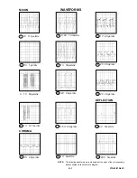
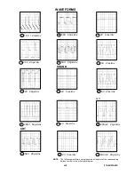
Page 37: ...esponding balloon number in the schematic diagram NOTE 2 1V 1µs div 3 1V 50µs div 4 1V 0 1ms div CHROMA 7 1V 20µs div 8 0 5V 10ms div 9 1V 50µs div 10 2V 20µs div 12 1V 2µs div 11 0 5V 20µs div 13 1V 20µs div 14 2V 20µs div 15 2V 20µs div 16 2V 5ms div DEFLECTION 17 20V 5ms div H 1 27A45 27A45C ...

Page 38: ...ber in the schematic diagram NOTE 18 10V 10ms div 19 20V 20µs div 20 2V 20µs div 21 200V 50µs div 37 50V 20µs div 38 50V 20µs div 39 50V 20µs div SOUND 22 2V 5ms div 23 2V 5ms div 24 2V 5ms div 25 2V 5ms div 26 5V 2ms div 27 5V 2ms div 28 200mV 20µs div 29 200mV 20µs div AV CRT H 2 27A45 27A45C ...

Page 39: ...CB ASS Y 109 112 112 MECHANICAL EXPLODED VIEW I 1 101B 101C 101E 101A 203 203 101F 203 101D 203 101 101G 101G 101G 201 201 201 201 201 203 107 102A 102C 102B 102B 201 201 102 111 PCB010 MAIN PCB ASS Y 207 204 205 206 103 206 110 105 104 207 27A45 ...

Page 40: ...Y 109 124 124 124 124 MECHANICAL EXPLODED VIEW I 2 101B 101C 101E 101A 203 203 101F 203 101D 203 101 108 101G 101G 101G 201 201 201 201 201 203 107 102A 102C 102B 102B 201 201 102 111 PCB010 MAIN PCB ASS Y 207 204 205 206 103 206 110 105 104 207 27A45C ...

Page 41: ...MECHANICAL EXPLODED VIEW PACKING DIAGRAM I 3 121 122 123 TM101 117 116 114 113 118 119 115 115 27A45 27A45C ...

Page 42: ...WIRE 110 BZ710260 899HV3T000 HOLDER ANODE WIRE 111 AE006143 726000A094 SHEET CRT SERVICEMAN 112 AD302158 800WR0A002 SHEET CRT SUPPORT 113 AE006929 723000C861 SHEET BAR CODE 114 AE006145 791WHAA116 FILM BAG 115 AD301626 792WHA0416 PACKAGE TOP 116 AD301627 792WHA0417 PACKAGE BOTTOM 117 AE006930 793WCDC667 GIFT BOX 118 AE000232 795WCA0665 PAD 378x1114 119 AE006147 795WCDA014 PAD 120 AE006931 A3S20229...

Page 43: ...CSA 109 AD300768 762WPA0009 HOLDER CRT WIRE 110 BZ710260 899HV3T000 HOLDER ANODE WIRE 111 AE006143 726000A094 SHEET CRT SERVICEMAN 113 AE006144 723000C811 SHEET BAR CODE 114 AE006145 791WHAA116 FILM BAG 115 AD301626 792WHA0416 PACKAGE TOP 116 AD301627 792WHA0417 PACKAGE BOTTOM 117 AE006146 793WCDC594 GIFT BOX 118 AE000232 795WCA0665 PAD 378x1114 119 AE006147 795WCDA014 PAD 120 AE006148 A3S2012975 ...

Page 44: ...K OHM 2W R805 BZ210050 R3X18A123J R METAL OXIDE 12K OHM 2W R807 BZ210050 R3X18A123J R METAL OXIDE 12K OHM 2W R1014 AE006741 R00204821J RC 820 OHM 1 4W CAPACITORS C156 AE004040 P6M900105J CMPL 1 UF 50V TF C408 BZ110032 E5EZF3102M CE 1000 UF 25V C412 AD301599 P4N8FJ272H CMPP 0 0027UF 1 25KV C413 AD301977 E0ELF4102M CE 1000 UF 35V C418 AE001019 P4J7F3434J CMPP 0 43 UF 250V PMS C420 AD300723 P4N8FJ153...

Page 45: ...S133T 77 D520 BZ410006 D1VT001330 DIODE SILICON 1SS133T 77 D523 AD300671 D97U01801B DIODE ZENER MTZJ18B T 77 D524 BZ410006 D1VT001330 DIODE SILICON 1SS133T 77 D525 BZ410094 D97U01501B DIODE ZENER MTZJ15B T 77 D528 BZ410021 D97U05R61B DIODE ZENER MTZJ5 6B T 77 D601 BZ410006 D1VT001330 DIODE SILICON 1SS133T 77 D602 BZ410058 D97U08R21B DIODE ZENER MTZJ8 2B T 77 D604 AD300070 D97U01201B DIODE ZENER MT...

Page 46: ...5S_Y_RTK Q801 BZ510100 TCATC3199Y TRANSISTOR SILICON KTC3199_Y AT Q802 BZ510100 TCATC3199Y TRANSISTOR SILICON KTC3199_Y AT Q803 BZ510100 TCATC3199Y TRANSISTOR SILICON KTC3199_Y AT Q804 BZ510091 TCA0042170 TRANSISTOR SILICON KTC4217 O Y Q805 BZ510091 TCA0042170 TRANSISTOR SILICON KTC4217 O Y Q806 BZ510091 TCA0042170 TRANSISTOR SILICON KTC4217 O Y Q901 BZ510108 TAAA1504SY TRANSISTOR SILICON KTA1504S...

Page 47: ...A3963WV2 3PD CP502 BZ614283 069S420110 CONNECTOR PCB SIDE A1561WV2 2P CP507 BZ614016 069W01001A CONNECTOR PCB SIDE 003P 2100 CP508 BZ614016 069W01001A CONNECTOR PCB SIDE 003P 2100 CP803 BZ614269 069S320010 CONNECTOR PCB SIDE A2361WV2 2P CP1001 AD301045 069S140419 CONNECTOR PCB SIDE A2502WV2 4P CP801A BZ614276 067U005049 WIRE HOLDER B2013H02 5P CP801B BZ614276 067U005049 WIRE HOLDER B2013H02 5P CP8...

Page 48: ...K OHM 2W R805 BZ210050 R3X18A123J R METAL OXIDE 12K OHM 2W R807 BZ210050 R3X18A123J R METAL OXIDE 12K OHM 2W R1014 AE006741 R00204821J RC 820 OHM 1 4W CAPACITORS C156 AE004040 P6M900105J CMPL 1 UF 50V TF C408 BZ110032 E5EZF3102M CE 1000 UF 25V C412 AD301599 P4N8FJ272H CMPP 0 0027UF 1 25KV C413 AD301977 E0ELF4102M CE 1000 UF 35V C418 AE001019 P4J7F3434J CMPP 0 43 UF 250V PMS C420 AD300723 P4N8FJ153...

Page 49: ...S133T 77 D520 BZ410006 D1VT001330 DIODE SILICON 1SS133T 77 D523 AD300671 D97U01801B DIODE ZENER MTZJ18B T 77 D524 BZ410006 D1VT001330 DIODE SILICON 1SS133T 77 D525 BZ410094 D97U01501B DIODE ZENER MTZJ15B T 77 D528 BZ410021 D97U05R61B DIODE ZENER MTZJ5 6B T 77 D601 BZ410006 D1VT001330 DIODE SILICON 1SS133T 77 D602 BZ410058 D97U08R21B DIODE ZENER MTZJ8 2B T 77 D604 AD300070 D97U01201B DIODE ZENER MT...

Page 50: ...S_Y_RTK Q801 BZ510100 TCATC3199Y TRANSISTOR SILICON KTC3199_Y AT Q802 BZ510100 TCATC3199Y TRANSISTOR SILICON KTC3199_Y AT Q803 BZ510100 TCATC3199Y TRANSISTOR SILICON KTC3199_Y AT Q804 BZ510091 TCA0042170 TRANSISTOR SILICON KTC4217 O Y Q805 BZ510091 TCA0042170 TRANSISTOR SILICON KTC4217 O Y Q806 BZ510091 TCA0042170 TRANSISTOR SILICON KTC4217 O Y Q901 BZ510108 TAAA1504SY TRANSISTOR SILICON KTA1504S_...

Page 51: ...A3963WV2 3PD CP502 BZ614283 069S420110 CONNECTOR PCB SIDE A1561WV2 2P CP507 BZ614016 069W01001A CONNECTOR PCB SIDE 003P 2100 CP508 BZ614016 069W01001A CONNECTOR PCB SIDE 003P 2100 CP803 BZ614269 069S320010 CONNECTOR PCB SIDE A2361WV2 2P CP1001 AD301045 069S140419 CONNECTOR PCB SIDE A2502WV2 4P CP801A BZ614276 067U005049 WIRE HOLDER B2013H02 5P CP801B BZ614276 067U005049 WIRE HOLDER B2013H02 5P CP8...

Page 52: ...TOSHIBA CORPORATION 1 1 SHIBAURA 1 CHOME MINATO KU TOKYO 105 8001 JAPAN ...

Reviews: