e-STUDIO160/200/250 COPYING PROCESS
3 - 2
December 2002 TOSHIBA TEC
3.2 Details of Copying Process
(1) Photosensitive Drum
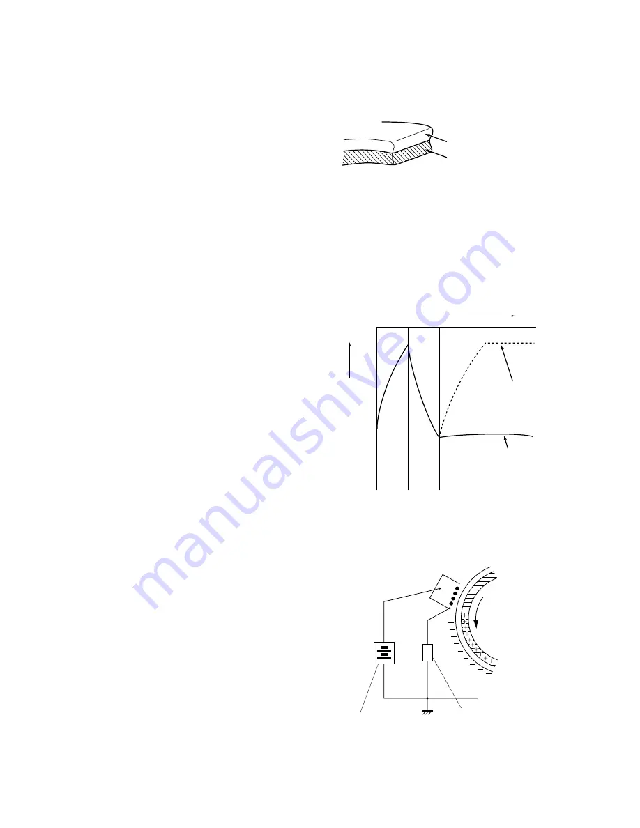
The photosensitive drum has two layers, an
outer and an inner layer. The outer layer is a
photoconductive layer that uses an organic
photoconductive carrier (OPC), and the inner
layer is an aluminum, conductive cylindrical
drum.
The resistance held by the drum material
changes (increases, decreases) according to
the strength of the light incident to the photo-
conductive carrier.
(Example)
• When incident light is strong, the resistance
decreases (photosensitive drum becomes a
carrier).
• When incident light is weak, the resistance
increases (photosensitive drum becomes an
insulator).
[Formation of Electrostatic Latent Image]
The minus potential on the drum surface cor-
responding to black areas of the original are
removed by the charging, scanning, printing
and discharging processes (described later),
and the minus potential remains on areas cor-
responding to white areas of the original.
The image on the drum resulting from this mi-
nus potential is called a “latent image” as it can-
not be seen directly by the human eye.
(2) Charging
"Charging" is the process of uniformly apply-
ing a charge to the surface of the photosensi-
tive drum.
The minus corona discharge of the charger wire
is controlled by the grid to charge the drum sur-
face to a uniform minus potential.
The drum surface potential is determined by
the potential of the grid, and the grid is deter-
mined by the grid control circuit inside the trans-
former.
Fig. 3-2-2
Electric potential of the photosensitive drum
Base
Photoconductive layer
Fig. 3-2-1 Structure of the photosensitive drum
03002
03003
0
– 500
– 1000
Time (t)
Black area of original
White area of original
Dis-
charge
process
Charg-
ing
process
Surface potential (V)
03004
Transformer
Main charger
Rotation of drum
Grid control circuit
Fig. 3-2-3
Summary of Contents for e-studio 160
Page 2: ... 2002 TOSHIBA TEC CORPORATION All rights reserved ...
Page 223: ...e STUDIO160 200 250 PCB BOARD 16 2 December 2002 TOSHIBA TEC 16 2 PWA F RLY 16 02 01 ...
Page 224: ...December 2002 TOSHIBA TEC 16 3 e STUDIO160 200 250 PC BOARD 16 3 PWA F PIF 16 03 01 ...
Page 226: ...December 2002 TOSHIBA TEC 16 5 e STUDIO160 200 250 PC BOARD 16 6 PWA F SLG 16 06 01 ...
Page 228: ...17 WIRE HARNESS CONNECTION DIAGRAMS 17 1 ...
Page 255: ...1 1 KANDA NISHIKI CHO CHIYODA KU TOKYO 101 8842 JAPAN ...


