13-2
e-STUDIO161 ELECTRICAL SECTION
2.Circuit descriptions
A. Main PWB (MCU)
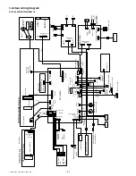
(1) Operation circuit
a. General
The operation circuit is composed of the key matrix circuit and the dis-
play matrix circuit.
b. Key matrix circuit
Select signals SELIN 1 - 3 are sent from the CPU of the MCU to the
selector in the operation circuit.
The signals detecting OFF/ON of the key are sent to the CPU as KIN 1 -
2.
c. Display circuit
The display is controlled by sending the data signal from the CPU of the
MCU, the clock signals, and the latch signals from the ASIC to the LED
driver in the operation circuit.
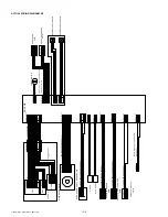
(2) I/F circuit
a. General
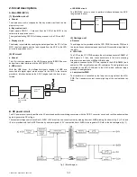
The I/F circuit is composed of the USB driver and the IEEE1284 driver,
and performs hard interface with the ASIC (MCU PWB).
b. USB circuit
With the USB driver, the differential signals (analog) of USB are
converted into digital signal, which are sent to the ASIC. In the reverse
procedure, interface between the ASIC (engine) and the host is per-
formed.
c. IEEE1284 circuit
The IEEE1284 driver is used to perform interface between the ASIC
(engine) and the host.
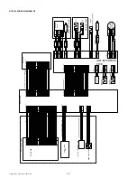
(3) Carriage unit
a. General
The carriage unit is provided with the CCD PWB, the inverter PWB, and
the lamps. It scans documents and transfers AD-converted image data to
the ASIC.
b. CCD PWB
The CCD on the CCD PWB employs the color image sensor uPD8861 of
5400 pixels x 3 lines, and scans documents in the main scanning
direction in the resolution of 600dpi/US letter size.
Image data scanned by the CCD are inputted to the AFE (AD9826), and
subject to CDS, amplification, and AD-conversion. Then digital data are
outputted to the MCU PWB and to the ASIC, which performs image
process of the digital data.
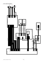
c. Lamp inverter PWB
The transformer is controlled by the lamp control signal from the MCU
PWB. The transformer output controls lighting of the cool cathode ray
tube.
USB driver
IC401
USB
connector
D -
D+
OE, RCV, VP, VM
Suspend, VMO
VPO
ASIC
Centronics
connector
IEEE1284
driver
IC403
ASIC
B. DC power circuit
The DC power circuit directly rectifies the AC power and performs switching-conversion with the DC/DC converter circuit, and rectifies and smoothes
again to generate a DC voltage.
The constant voltage control circuit is of +5VEN. +24V are of the non-control system by winding from the +5VEN winding. As shown in fig (1), +24V, and
+5V are provided with the ON/OFF function by external signals. +3.3V is outputted from +5VEN to the regulator IC. Refer to the block diagram, fig (1).
fig (1) Block diagram
[13]ELECTRICALSECTION.fm 2 ページ 2004年1月9日 金曜日 午後1時23分


