13-4
e-STUDIO161 ELECTRICAL SECTION
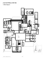
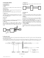
The control circuit is subject to negative feedback from the secondary
side as shown in fig (4). A photo coupler (PC002) is employed to insulate
between the primary side and the secondary side to feed back the
control signal to the primary side.
When the output voltage is increased by energy transmission from T001,
the voltage detected by R109 and R111 is compared with the reference
voltage of IC102. When it exceeds the reference voltage, the current
flowing through IC102 (that is, the photo diode current of PC002) is
increased and transmitted to the primary side. Then the potential at the
feedback pin (2 pin) of IC102 is decreased to control Q001. Therefore,
the change in the output voltage on the secondary side is passed
through IC102 and PC002 to control Q001, stabilizing the output voltage.
(4) Overcurrent protection circuit (Primary side)
The inverter circuit of the primary side is connected with the current
detection resistor R012. When an overcurrent occurs in the secondary
side, the current flowing through the primary side inverter Q001 is
increased. The current is detected by R012, and passed through R013 to
IC002 overcurrent restricting pin (3 pin) to turn OFF Q002, shutting off all
power. To resupply the power, turn off and on the power. Refer to fig (4).
(5) Rectifying/smoothing circuit (+5V)
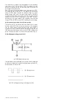
fig (6) Rectifying/smoothing circuit
The high frequency pulse generated by the inverter circuit is decreased
by the converter transformer, rectified by the high frequency diode D103,
and smoothed by C103 and C104.
fig (7) +5V rectifying/smoothing circuit voltage waveform
[13]ELECTRICALSECTION.fm 4 ページ 2004年1月9日 金曜日 午後1時23分

