background image

SECTION 4

PARTS LIST

SAFETY PRECAUTION

The parts identified by ! (     ) mark are critical for safety.  Replace only with part number specified.
The mounting position of replacement is to be identical with originals.
The substitute replacement parts which do not have the same safety characteristics as specified in the parts list may create
shock, fire or other hazards.

NOTICE

The part number must be used when ordering parts in order to assist in processing, be sure to include the model number
and description.

ABBREVIATIONS


Integrated Circuit (IC)


Capacitor (Cap)

     •  Capacitance Tolerance (for Nominal Capacitance more than 10pF)

P

+ 100

0

Symbol

Tolerance %

B

± 0.1

C

± 0.25

D

± 0.5

F

± 1

G

± 2

J

± 5

K

± 10

M

± 20

N

± 30

V

+ 20

– 10

W

+ 100

  – 10

U

+ 75

– 10

Q

+ 30

– 10

T

+ 50

– 10

Symbol

Tolerance %

X

+ 40

– 20

Y

+ 150

  – 10

Z

+ 80

– 20

Ex. 10µF J = 10µF ± 5%

Symbol

Tolerance pF

B

± 0.1

C

± 0.25

D

± 0.5

F

± 1

G

± 2

Ex. 10pF G = 10pF ± 2pF

M

± 20

Symbol

Tolerance %

B

± 0.1

C

± 0.25

D

± 0.5

F

± 1

G

± 2

J

± 5

K

± 10

Ex. 470

J = 470

± 5%

Table 4-2-1

Table 4-2-2

Table 4-3-1

     •  Capacitance Tolerance (for Nominal Capacitance 10pF or less)

  Resistor (Res)

     •  Resistance tolerance

SECTION 4

P

ARTS LIST

Summary of Contents for HD-E1KE

Page 1: ...s are classified as green products 1 as indicated by the underlined serial numbers This Service Manual describes replacement parts for the green products When repairing these green product s use the part s described in this manual and lead free solder 2 For 1 and 2 see the next page Rev 01 ...

Page 2: ...ment of parts is not only confined to manufacture The same green parts used in manufacture must also be used as replacement parts 2 LEAD FREE SOLDER This product is manufactured using lead free solder as a part of a movement within the con sumer products industry at large to be environmentally responsible Lead free solder must be used in the servicing and repair of this product WARNING This produc...

Page 3: ... characteristics such as inflammability voltage resistance etc therefore use only replacement parts that have these same characteristics Use only the specified parts when the mark is include in a circuit diagram or parts list Parts mounting and routing of the wiring should be the same as that used originally For safety purposes insulating materials such as tubing or tape is sometimes used and prin...

Page 4: ...d the following values for a c U1 35 V peak and U2 0 35 V perk for d c U1 1 0 V NOTE 5 The limit values of U2 0 35 V peak for a c and U1 1 0 V for d c correspond to the values 0 7mA peak a c and 2 0 mA 2 0mA d c The limit value U1 35 V peak for a c corresponds to the value 70mA peak a c for frequencies greater than 100 kHz Annex D normative Measuring network for TOUCH CURRENTS A B Test TERMINALS R...

Page 5: ...atic diagram and the parts list Before replacing any of these components read the parts list in this manual carefully The use of substitute replacement parts which do not have the same safety characteristics as specified in the parts list may create shock fire or other hazards The lightning flash with arrowhead symbol within an equilateral triangle is intended to alert the user to the presence of ...

Page 6: ...ures manufactured under license from Dolby Laboratories Dolby and the double D symbol are trademarks of Dolby Laboratories DTS features manufactured under license from Digital Theater Systems Inc U S Pat No s 5 451 942 5 956 674 5 974 380 5 978 762 6 226 616 6 487 535 and other U S and world wide patents issued and pending DTS and DTS Digital Surround are registered trademarks of Digital Theater S...

Page 7: ...agram 4 2 3 Front Switch USB Circuit Diagram 4 3 ATAPI Conversion Circuit Diagram 4 4 Main Circuit Diagram 4 4 1 AV Output Circuit Diagram 4 4 2 Timer Circuit Diagram 5 PC BOARDS 5 1 Front FIP PC Board 5 2 Power Switch PC Board 5 3 Front Switch USB PC Board 5 4 ATAPI PC Board CONTENTS SECTION 1 GENERAL DESCRIPTIONS 1 OPERATING INSTRUCTIONS 1 REPLACEMENT OF MECHANICAL PARTS 1 1 Front Panel Front PC...

Page 8: ...SECTION 1 GENERAL DESCRIPTIONS 1 OPERATING INSTRUCTIONS Please refer to the owner s manual about the contents SECTION 1 GENERAL DESCRIPTIONS ...

Page 9: ... OF MAIN PARTS 2 1 Location of Main Parts Fig 1 2 1 2 2 Location of PC Boards Fig 1 2 2 FAN DVD DRIVE Main PC board Power PC board ATAPI PC board Front FIP PC board Front switch USB PC board Power switch PC board ...

Page 10: ... as required Many screws are used inside the unit To prevent the screws from missing or dropping etc always use a magnetized screwdriver in servicing Several kinds of screws are used and some of them need special cautions That is take care of the tapping screws securing molded parts and fine pitch screws used to secure metal parts If they are used improperly the screw holes will be easily damaged ...

Page 11: ...1 2 Main Power PC Boards Fig 2 1 2 POWER PC BOARD MAIN PC BOARD 1 1 7 7 3 5 9 11 10 9 9 9 10 10 9 12 6 2 4 4 8 FAN ...

Page 12: ...1 3 DVD Drive Fig 2 1 3 DVD DRIVE ATAPI PC BOAD 7 2 1 6 3 4 5 1 1 ...

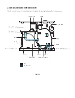
Page 13: ...ring to its original state by using the diagram below as a reference Fig 2 2 1 Flexible cable Tape Front panel DVD DRIVE W003 Main PC board Power PC board Power switch PC board FAN W102 W104 W101 W002 Front FIP PC board W001 Front switch USB PC board ATAPI PC board W103 W004 ...

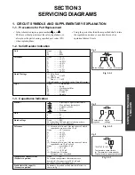
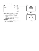
Page 14: ...c and film capacitors of which capacitance are more than 10 pF None 5 or more B 0 1 C 0 25 D 0 5 F 1 G 2 2 Ceramic plastic and film capacitors of which capacitance are 10 pF or less None more than 5 pF B 0 1 pF C 0 25 pF 3 Electrolytic Trimmer Tolerance is not described Temperature characteristic None SL Ceramic capacitor For others temperature characteristics are described For capacitors of 0 01 ...

Page 15: ...forms for CD DVD and RF shown in the circuit diagrams are obtained when a test disc is played back All voltage values except the waveforms are expressed in DC and measured by a digital voltmeter 1 6 Others The parts indicated with NC or KETU etc are not used in the circuits of this model Eg 4 Eg 5 Fig 3 1 4 Fig 3 1 5 Type name 10µ Type Tolerance ...

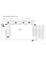
Page 16: ... K2 K1 EJECT SW D_LIGHT_LED E1 S2 SG10 SG9 SG8 SG7 14G 14G SG18 SG17 SG16 SG15 SG14 SG13 SG12 SG11 14G GND 14G 14G 14G 14G 14G GND 14G 14G 14G 14G 14G 14G 5V 5V 12V 12V 5V GND D1 VDD NC B_DA0 B_DA2 B_DIOR D_GND B_IORDY B_CS1 B_DASP B_CS0 B_DMACK D_GND B_INTRQ NC B_DA1 VEE 5V GND FL 5V GND F 14G 14G 14G 14G 14G GND GND GND PS_ON VCC 3 3V GND VCC 3 3V B 5V VCC 5V GND DD9 EJECT_SW TRAY_STATUS NC GND ...

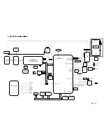
Page 17: ...IC1 UART UART1 N Wire interface 2 Vr5500 and V850 EJTAG interface 32bit DDR2 SDRAM interface Video output CY CB CR DVO0 IEC60958 Output DAO0 0 4 SYSTEM CLOCK HDMI Tx SiI9030 Timer uCOM 78F0535 Front Unit Audio DAC PCM1755 SPI OP Amp NJM4580 Video Driver MM1757 Video output SY SC Buffer 100MHz 3 3V 5VTrans FL Driver Power Suplly 48MHz 33MHz 33MHz 33MHz 256MB DDR2 SDRAM 1Gb 2 16bit DDR2 SDRAM BCK LR...

Page 18: ...Fig 3 4 1 4 CIRCUIT DIAGRAMS 4 1 Power Supply Circuit Diagram ...

Page 19: ...4 2 Front Circuit Diagram 4 2 1 Front FIP Circuit Diagram Fig 3 4 2 ...

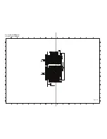
Page 20: ...Use Not use 4 2 2 Power Switch Circuit Diagram Fig 3 4 3 ...

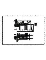
Page 21: ...4 2 3 Front Switch USB Circuit Diagram Use Do vout guard at GND Not use Not use Not use Fig 3 4 4 ...

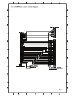
Page 22: ...Fig 3 4 5 4 3 ATAPI Conversion Circuit Diagram ...

Page 23: ...V21 EV22 EV25 EV23 EV02 EV03 10uF16V CA12 100uF16V CA18 GND 100uF16V CV12 F0 1u CV04 F0 1u CV02 F0 1u CV03 100uF16V CV17 EV12 2 2k RV24 RV13 100 QV07 2SC2712Y F0 1u CV01 QV08 2SC2712Y 2 2k RV44 RV16 100 QV06 NC QV05 NC NC RV20 RV10 NC NC RV22 RV03 NC QV09 2SC2712Y RV18 100 2 2k RV45 JV03 YKF 45 3011 12 13 14 11 10 9 8 7 6 5 4 3 2 1 EV38 EV39 EV40 EV41 EV42 EV43 EV54 EV55 EV56 EV57 EV58 EV59 EV60 D...

Page 24: ...5 AV_TxD 46 AVref 47 AGND 48 P5V_SEN 49 P3V_SEN 50 P12V_SEN 51 CVBS YUVX 52 CEC 53 VMUTE2 54 SEL_I P 55 S1_ASP 56 ONVCC_M5P 57 DRISCK 58 DRI_IN D T 59 DRU_OUT T D 60 DRI_CS 61 PWR_LED 62 BUZZER 63 RTC_OUT 64 R751 10k R752 10k R785 100 R773 100 R733 100 CLK_32K R703 100 R711 100 R714 10K R715 10K R720 100 R723 100 PWROK M5P R734 100 USBON0 M5P R735 100 USBOC0 P5N R736 100 USBOC1 P5N SHRST M5N R727 ...

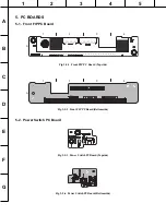
Page 25: ...nt FIP PC Board Bottom side 5 2 Power Switch PC Board Fig 3 5 1 Front FIP PC Board Top side Fig 3 5 3 Power Switch PC Board Top side Fig 3 5 4 Power Switch PC Board Bottom side A100 CN104 CN105 W173 1 2 3 4 A 1 2 3 4 A CN101 D121 D122 S115 C118 Q101 Q102 R101 R102 R146 R147 ...

Page 26: ...S103 S104 S107 S108 S109 S116 W103 W172 1 2 3 4 5 A C100 C101 C112 FL101 FL102 L101 L102 L103 L104 L105 R103 R104 R105 R106 R107 R108 R110 R148 R149 RJ01 RJ02 RJ03 1 2 3 4 5 A Fig 3 5 6 Front Switch USB PC Board Bottom side 5 4 ATAPI PC Board 1 2 A Fig 3 5 7 ATAPI PC Board Top side 1 2 A Fig 3 5 8 ATAPI PC Board Bottom side ...

Page 27: ...in processing be sure to include the model number and description ABBREVIATIONS Integrated Circuit IC Capacitor Cap CapacitanceTolerance for Nominal Capacitance more than 10pF P 100 0 Symbol Tolerance B 0 1 C 0 25 D 0 5 F 1 G 2 J 5 K 10 M 20 N 30 V 20 10 W 100 10 U 75 10 Q 30 10 T 50 10 Symbol Tolerance X 40 20 Y 150 10 Z 80 20 Ex 10µF J 10µF 5 Symbol TolerancepF B 0 1 C 0 25 D 0 5 F 1 G 2 Ex 10pF...

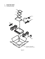
Page 28: ...1 EXPLODED VIEWS 1 1 Packing Assembly Fig 4 1 1 Note The shape of the packing material is sometimes different Z001A Z005 Z010 Z011 Z001 Z006 Z002 ...

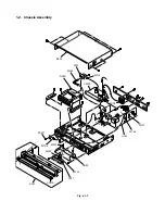
Page 29: ...1 2 Chassis Assembly Fig 4 1 2 D A B C D A B C B300 ATA1 PWR1 W101 W104 U001 USB1 W002 FRT1 A001A A001 W003 W001 W103 PSW1 FAN1 W102 W004 RAM1 ...

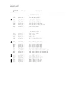
Page 30: ...0 HD DVD DRIVE SD E802A W001 P000477420 FFC 12P L102 MAIN FRONT W002 P000477430 FFC 20P L102 MAIN FRONT W003 P000477440 FFC 16P L102 MAIN FRONT W004 P000477450 FFC 40P L242 MAIN DRIVE W101 P000477530 WIRE CABLE ZHR 9P L300 MAIN USB W102 P000477540 WIRE CABLE PHR 6P L100 POWER ATAPI W103 P000477550 WIRE CABLE ZHR 4P L380 MAIN PWRSW W104 P000477560 WIRE CABLE PHR 4P L260 MAIN POWER Z001 P000354930 C...

Page 31: ... green 1 0Vp p 75Ω Sync signal negative Pin jack x 1 system PB PR output blue red 0 7Vp p 75Ω Pin jack x 1 system each 2 0V rms 2 2kΩ or below pin jack L R x 1 system Optical connector x 1 system 100BASE TX 10BASE T x 1 EXTENSION port x 2 systems 19 pin Wireless remote control SE R0252 Temperature 41 F 95 F 5 C 35 C Position Horizontal Quartz monthly deviation approximately 30 seconds SPECIFICATIO...

Page 32: ...1 1 SHIBAURA 1 CHOME MINATO KU TOKYO 105 8001 JAPAN ...

Reviews: