2-5
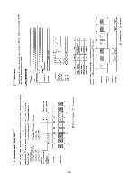
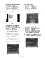
1-2-1. Sub Carrier Frequency Adjustment
Screen display:
01 INT SC
Test equipment: Frequency counter
Test point:
TL01/Driver PC board
Adjusting point:
DATA UP/DOWN
Specification:
3.579545 MHz ± 10 Hz
Note:
External sync mode is not set.
Fig. 10
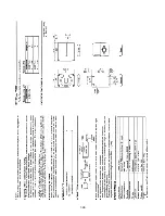
1-2-2. R - Y Carrier Balance Adjustment
Screen display:
02 R - Y CAR BAL
Test equipment: Vector scope (MAX GAIN)
Test point:
VIDEO OUT
Adjusting point:
DATA UP/DOWN
1. Set the luminance spot of the vector scope
at its center with the DATA buttons.
1-2-3. B - Y Carrier Balance Adjustment
Screen display:
03 B - Y CAR BAL
Test equipment: Vector scope (MAX GAIN)
Test point:
VIDEO OUT
Adjusting point:
DATA UP/DOWN
1. Set the luminance spot of the vector scope
at its center with the DATA buttons.
2. Repeat the items 1-2-2 and 1-2-3 to set the
luminance spot to the center of the vector
scope.
1-2-4. REF G Adjustment
Screen display:
04 REF G
Test equipment: WFM (LPF mode)
Test point:
VIDEO OUT
Adjusting point:
DATA UP/DOWN
Specification:
60 ± 1 IRE
1. Adjust the white level of the waveform to 60
± 1 IRE with the DATA buttons.
1-2-5. REF R , REF B Adjustment
Screen display:
05 REF R, REF B
Test equipment: Vector scope (MAX GAIN)
Test point:
VIDEO OUT
Adjusting point:
RL50, RL51/Driver PC board
1. Set the luminance spot of the vector scope
at its center by adjusting at RL50, RL51.
Note:
The black and white luminance spots appear.
Adjust either of the two which is moved by the
RL50, RL51.
DC/DC
TL01
Summary of Contents for IK-TU51CU
Page 4: ...1 1 SECTION 1 GENERAL DESCRIPTION IK TU51CU ...
Page 5: ...1 2 ...
Page 6: ...1 3 ...
Page 7: ...1 4 ...
Page 8: ...1 5 ...
Page 9: ...1 6 ...
Page 10: ...1 7 ...
Page 11: ...1 8 ...
Page 12: ...1 9 ...
Page 13: ...1 10 ...
Page 14: ...1 11 ...
Page 15: ...1 12 ...
Page 16: ...1 13 ...
Page 17: ...1 14 ...
Page 18: ...1 15 ...
Page 19: ...1 16 ...
Page 20: ...1 17 ...
Page 21: ...1 18 ...
Page 22: ...1 19 ...
Page 23: ...1 20 ...
Page 24: ...1 21 ...
Page 25: ...1 22 ...
Page 26: ...1 23 ...
Page 27: ...1 24 ...
Page 28: ...1 25 JK TU52H ...
Page 29: ...1 26 ...
Page 30: ...1 27 JK TU53H ...
Page 31: ...1 28 ...
Page 41: ...3 2 1 2 Packing Assembly JK TU52H JK TU53H Y110 A701 A702 ...
Page 43: ...3 4 1 4 Camera Head Assembly JK TU52H A110A A110A A116A A111A A111 A116 A110 A113 PF01 PF01 ...
Page 44: ...3 5 1 5 Camera Head Assembly JK TU53H A113 A110 A110A PF01 PF01A PF01 A111 A111A A111A ...
Page 54: ...4 2 1 3 Rear PC Board IK 528A Component Side Soldering Side ...
Page 55: ...4 3 1 4 Driver PC Board Component Side ...
Page 56: ...4 4 Soldering Side ...
Page 57: ...4 5 1 5 DSP PC Board Component Side ...
Page 58: ...4 6 Soldering Side ...
Page 59: ...4 7 2 BLOCK DIAGRAMS 2 1 Power Supply Block Diagram ...
Page 60: ...2 2 TG SG Block Diagram 4 8 4 9 ...
Page 61: ...2 3 Pre Process Block Diagram 4 10 4 11 ...
Page 62: ...2 4 ENC Output Block Diagram 4 12 4 13 ...
Page 63: ...2 5 DSP Block Diagram 4 14 4 15 ...
Page 64: ...2 6 Memory Block Diagram 4 16 4 17 ...
Page 65: ...4 1 2 7 Auto Block Diagram 4 18 ...
Page 66: ...4 2 2 8 D Out Block Diagram 4 19 ...
Page 67: ...4 20 4 21 3 CIRCUIT DIAGRAMS 3 1 Overall Wiring Diagram ...
Page 68: ...4 22 4 23 3 2 Power Supply Circuit Diagram ...
Page 69: ...3 3 TG Circuit Diagram 4 24 4 25 4 26 ...
Page 70: ...4 27 4 28 4 29 3 4 SG Circuit Diagram ...
Page 71: ...4 30 4 31 3 5 Pre Process Circuit Diagram ...
Page 72: ...4 32 4 33 4 34 3 6 ENC Circuit Diagram ...
Page 73: ...4 35 4 36 3 7 Output Circuit Diagram ...
Page 74: ...4 37 4 38 4 39 3 8 DSP Circuit Diagram ...
Page 75: ...4 40 4 41 4 42 3 9 Memory Circuit Diagram ...
Page 76: ...4 43 4 44 3 10 Auto Circuit Diagram ...
Page 77: ...4 45 4 46 3 11 D Out Circuit Diagram ...
Page 78: ...4 1 3 12 Rear Circuit Diagram 4 47 ...
Page 79: ...SECTION 5 SPECIFICATIONS 1 SPECIFICAIONS IK TU51CU JK TU52H JK TU53H ...
Page 80: ......


