2-6
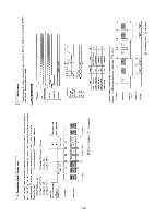
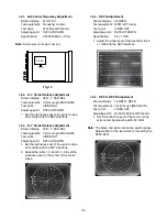
1-2-6. B - Y Level Ajustment
Screen display:
06 B - Y LEVEL
Test equipment: Vector scope
Test point:
VIDEO OUT
Adjusting point:
RL52/Driver PC board
1. Overlap the burst signal on B - Y axis with
the PHASE control of the vector scope.
2. Adjust the R luminance spot to set it within
the mark with the GAIN control of the vector
scope.
3. Adjust the color luminance spot of YL to set
it within each mark by adjusting at RL52.
4. Confirm each color luminance spot (YL, CY,
G, MG, R, B) to set it within each mark .
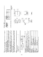
1-2-7. Color Adjustment
Screen display:
07 CHR LEVEL
Test equipment: WFM (BPF mode)
Test point:
VIDEO OUT
Adjusting point:
DATA UP/DOWN
Specification:
95 ± 2 IRE
1. Adjust the R amplitude on the waveform
monitor to 95 ± 2 IRE with the DATA buttons.
1-2-8. Burst Level Adjustment
Screen display:
08 BURST LEVEL
Test equipment: WFM (BPF mode),
Vector scope
Test point:
VIDEO OUT
Adjusting point:
DATA UP/DOWN
1. Adjust the burst level to 75% position of the
vector scope with the DATA buttons.
Or, adjust the burst level of the waveform
monitor to 40 ± 1 IRE with the DATA buttons.
1-2-9. ABB1 Adjustment
Screen display:
09 ABB1
1. Set the lens iris to close.
2. Push the DATA buttons.
3. The automatic black balance adjustment is
performed automatically and “ABB OK” is
displayed on the screen.
1-2-10. ABB2 Adjustment
Screen display:
11 ABB2
1. Set the lens iris to close.
2. Push the DATA buttons.
3. The automatic black balance adjustment is
performed automatically, and “ABB OK” is
displayed on the screen.
1-2-11. Area Size Adjustment
Test equipment: WFM (1
µ
s mode)
Test point:
VIDEO OUT
Adjusting point:
CA50/DSP PC board
Specification:
4.5
µ
s ± 400 ns
1. Set SA01 on the DSP PC board to NORM
side.
2. Set the lens iris to close.
3. Push the DISP button twice to display the
INDEX screen.
4. Push the PAGE button to display the SHUT-
TER screen.
5. Set the MODE to AUTO with the DATA
buttons.
6. Set the “
→
” cursor to AREA position with the
MENU DOWN button and set to PRESET A
with the DATA buttons.
7. Set the “
→
” cursor to AREA DISP position
with the MENU DOWN button.
8. Set the screen to the AREA screen by
pushing the DATA buttons.
9. Adjust the portion A to obtain 4.5
µ
s ± 400
ns by adjusting CA50.
Summary of Contents for IK-TU51CU
Page 4: ...1 1 SECTION 1 GENERAL DESCRIPTION IK TU51CU ...
Page 5: ...1 2 ...
Page 6: ...1 3 ...
Page 7: ...1 4 ...
Page 8: ...1 5 ...
Page 9: ...1 6 ...
Page 10: ...1 7 ...
Page 11: ...1 8 ...
Page 12: ...1 9 ...
Page 13: ...1 10 ...
Page 14: ...1 11 ...
Page 15: ...1 12 ...
Page 16: ...1 13 ...
Page 17: ...1 14 ...
Page 18: ...1 15 ...
Page 19: ...1 16 ...
Page 20: ...1 17 ...
Page 21: ...1 18 ...
Page 22: ...1 19 ...
Page 23: ...1 20 ...
Page 24: ...1 21 ...
Page 25: ...1 22 ...
Page 26: ...1 23 ...
Page 27: ...1 24 ...
Page 28: ...1 25 JK TU52H ...
Page 29: ...1 26 ...
Page 30: ...1 27 JK TU53H ...
Page 31: ...1 28 ...
Page 41: ...3 2 1 2 Packing Assembly JK TU52H JK TU53H Y110 A701 A702 ...
Page 43: ...3 4 1 4 Camera Head Assembly JK TU52H A110A A110A A116A A111A A111 A116 A110 A113 PF01 PF01 ...
Page 44: ...3 5 1 5 Camera Head Assembly JK TU53H A113 A110 A110A PF01 PF01A PF01 A111 A111A A111A ...
Page 54: ...4 2 1 3 Rear PC Board IK 528A Component Side Soldering Side ...
Page 55: ...4 3 1 4 Driver PC Board Component Side ...
Page 56: ...4 4 Soldering Side ...
Page 57: ...4 5 1 5 DSP PC Board Component Side ...
Page 58: ...4 6 Soldering Side ...
Page 59: ...4 7 2 BLOCK DIAGRAMS 2 1 Power Supply Block Diagram ...
Page 60: ...2 2 TG SG Block Diagram 4 8 4 9 ...
Page 61: ...2 3 Pre Process Block Diagram 4 10 4 11 ...
Page 62: ...2 4 ENC Output Block Diagram 4 12 4 13 ...
Page 63: ...2 5 DSP Block Diagram 4 14 4 15 ...
Page 64: ...2 6 Memory Block Diagram 4 16 4 17 ...
Page 65: ...4 1 2 7 Auto Block Diagram 4 18 ...
Page 66: ...4 2 2 8 D Out Block Diagram 4 19 ...
Page 67: ...4 20 4 21 3 CIRCUIT DIAGRAMS 3 1 Overall Wiring Diagram ...
Page 68: ...4 22 4 23 3 2 Power Supply Circuit Diagram ...
Page 69: ...3 3 TG Circuit Diagram 4 24 4 25 4 26 ...
Page 70: ...4 27 4 28 4 29 3 4 SG Circuit Diagram ...
Page 71: ...4 30 4 31 3 5 Pre Process Circuit Diagram ...
Page 72: ...4 32 4 33 4 34 3 6 ENC Circuit Diagram ...
Page 73: ...4 35 4 36 3 7 Output Circuit Diagram ...
Page 74: ...4 37 4 38 4 39 3 8 DSP Circuit Diagram ...
Page 75: ...4 40 4 41 4 42 3 9 Memory Circuit Diagram ...
Page 76: ...4 43 4 44 3 10 Auto Circuit Diagram ...
Page 77: ...4 45 4 46 3 11 D Out Circuit Diagram ...
Page 78: ...4 1 3 12 Rear Circuit Diagram 4 47 ...
Page 79: ...SECTION 5 SPECIFICATIONS 1 SPECIFICAIONS IK TU51CU JK TU52H JK TU53H ...
Page 80: ......


