background image

CRT

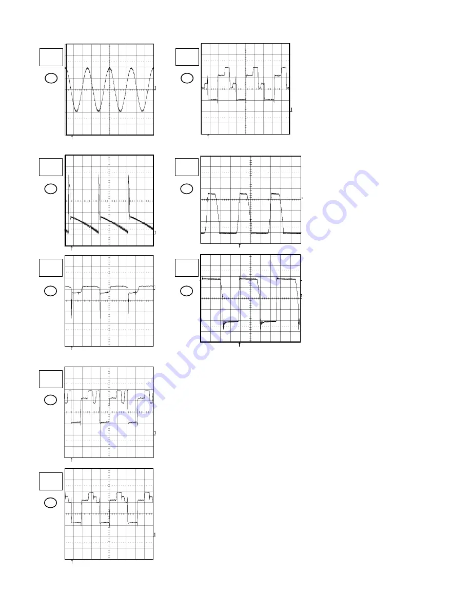
WAVEFORMS

The following waveforms were measured at the point of the corresponding
balloon number in the schematic diagram.

NOTE:

POWER

DEFLECTION

47

48

49

46

44

45

43

42

POWER ON

1ms

200mV

POWER ON

5ms

10.0V

POWER ON

20

µ

s

5.0V

POWER ON

20

µ

s

50V

POWER ON

20

µ

s

50V

STANDBY

5

µ

s

5.0V

STANDBY

5

µ

s

5.0V

POWER ON

20

µ

s

50V

H-3

Summary of Contents for MD13N1/R

Page 1: ...SERVICE MANUAL COLOR TELEVISION DVD VIDEO PLAYER MD13N1C FILE NO 140 200324 MD13N1R DOCUMENT CREATED IN JAPAN Jun 2003 ...

Page 2: ...OLS ADJUSTMENTS OR THE PERFORMANCE OF PROCEDURES OTHER THAN THOSE SPECIFIED HEREIN MAY RESULT IN HAZARDOUS RADIATION EXPOSURE TO PREVENT DIRECT EXPOSURE TO LASER BEAM DO NOT TRY TO OPEN THE ENCLOSURE VISIBLE LASER RADIATION MAY BE PRESENT WHEN THE ENCLOSURE IS OPENED DO NOT STARE INTO BEAM Location of the required Marking The rating sheet and the safety caution are on the rear of the unit CERTIFIC...

Page 3: ...ether there are the portions which are deteriorated around the serviced places serviced or not Check the insulation between the antenna terminal or external metal and the AC cord plug blades And be sure the safety of that INSULATION CHECK PROCEDURE 1 2 3 4 Unplug the plug from the AC outlet Remove the antenna terminal on TV and turn on the TV Insulation resistance between the cord plug terminals a...

Page 4: ...nto the outlet try reversing the plug If the plug should still fail to fit contact your electrician to replace your obsolete outlet Do not defeat the safety purpose of the polarized plug If your unit is equipped with a 3 wire grounding type plug a plug having a third grounding pin this plug will only fit into a grounding type power outlet This too is a safety feature If you are unable to insert th...

Page 5: ...ire HEADPHONES When you use the headphones keep the volume at a moderate level If you use the headphones continuously with high volume sound it may cause hearing damage LASER BEAM Do not look into the opening of the disc tray or ventilation opening of the product to see the source of the laser beam It may cause sight damage DISC Do not use a cracked deformed or repaired disc These discs are easily...

Page 6: ...steps below NB The above procedure will reset ALL of the player s settings to the default factory state Turn Unit ON Set the DVD to the Stop Mode Set the VOLUME to minimum Press and hold the VOL DOWN button on the front panel Simultaneously press and hold the 4 key on the remote control unit Hold both keys for more than 1 second The On Screen Display message INITALIZE5 COMPLETE will appear The Tra...

Page 7: ...TABLE OF CONTENTS GENERAL SPECIFICATIONS DISASSEMBLY INSTRUCTIONS 1 REMOVAL OF MECHANICAL PARTS AND P C BOARDS 2 REMOVAL OF DVD DECK PARTS 3 REMOVAL OF ANODE CAP 4 REMOVAL AND INSTALLATION OF FLAT PACKAGE IC SERVICE MODE LIST CONFIRMATION OF USING HOURS WHEN REPLACING EEPROM MEMORY IC ELECTRICAL ADJUSTMENTS BLOCK DIAGRAMS DVD ST SOLUTION TV POWER PRINTED CIRCUIT BOARDS DVD AV CRT SCHEMATIC DIAGRAM...

Page 8: ... CD Slow speed Fwd 1 8 1 2 times Actual Rev 1 8 1 2 times Actual G 3 Tuning Broadcasting System US System M System Tuner and System 1Tuner Receive CH Destination US w CATV Tuning System F Synth Input Impedance VHF UHF 75 Ohm CH Coverage 2 69 4A A 5 A 1 A I J W W 1 W 84 Intermediate Picture FP 45 75MHz Frequency Sound FS 41 25MHz FP FS 4 50MHz Preset CH No Stereo Dual TV Sound US Stereo Tuner Sound...

Page 9: ...ness Yes Contrast Yes Color Yes Tint Yes Sharpness Yes Sound No Bass No Treble No Balance No CH Yes TV CATV Yes Add Delete Yes Auto CH Memory Yes Option Yes V Chip Yes Language Yes Open Yes Close Yes Clock No Clock Set No On Off Timer No Sleep Timer Yes CH AV LINE DVD Yes Stereo Audio Output Yes Bilingual No SAP Yes Caption Text Yes Auto Search Position No Game Yes Volume Yes Mute Yes A3 2 ...

Page 10: ...ng Level Yes Open Yes Close Yes No disc Yes Reading Yes Play Yes Still Pause Yes Stop Yes Prohibit Mark Yes Step Yes Skip Yes Skip Yes Random Yes CD Repeat Yes Slow Yes Slow Yes Search Yes Search Yes Jump Yes Resume Yes Title No Yes Chapter No Yes Track No Yes Time Yes Sub Title No Yes Angle No Yes Vocal On Off No Audio No Yes Audio Stereo L R Yes Video CD Zoom Yes Marker No No Program Play Back Y...

Page 11: ...0 Yes Play Yes Stop Yes Search Yes Search Yes Skip Yes Skip Yes Slow Yes Slow Yes Pause Yes Call Yes TV DVD Yes Cancel Yes Audio Select Yes Angle Yes Subtitle Yes Top Menu Yes Set up Menu Yes DVD Menu Yes Return Yes Up Set CH Up Yes Down Set CH Down Yes Left Select Vol Down Yes Right Select Vol Up Yes Select Enter Yes Play Mode Yes Closed Caption Yes Input Select Yes Repeat A B Yes Zoom Quick View...

Page 12: ...Jump No MP3 Playback No Digital Out Dolby Digital Yes MPEG Yes PCM Yes DTS Yes Down Mix Out Dolby Digital Yes DTS No Surround Tru Surround No Screen Saver No Audio DAC 192kHz 24bit G 14 Accessories Owner s Manual Language English w Guarantee Card Yes Buyer Model No MD13N1R Remote Control Unit Yes Battery Yes UM size x pcs UM 4 x 2 pcs OEM Brand No Rod Antenna No Poles No Terminal Loop Antenna No T...

Page 13: ...ter No VHF UHF Antenna Input F Type G 16 Set Size Approx W x D x H mm 362x365x382 G 17 Weight Net Approx 11 0kg 24 3lbs Gross Approx 12 5kg 27 6lbs G 18 Carton Master Carton No Content Sets Material Dimensions W x D x H mm Description of Origin Gift Box Yes Material Double White W Color Photo Label No Dimensions W x D x H mm 423x447x443 Design As Per Buyer s Description of Origin Yes Buyer Model N...

Page 14: ...s CD Slow speed Fwd 1 8 1 2 times Actual Rev 1 8 1 2 times Actual G 3 Tuning Broadcasting System US System M System Tuner and System 1Tuner Receive CH Destination US w CATV Tuning System F Synth Input Impedance VHF UHF 75 Ohm CH Coverage 2 69 4A A 5 A 1 A I J W W 1 W 84 Intermediate Picture FP 45 75MHz Frequency Sound FS 41 25MHz FP FS 4 50MHz Preset CH No Stereo Dual TV Sound US Stereo Tuner Soun...

Page 15: ...ness Yes Contrast Yes Color Yes Tint Yes Sharpness Yes Sound No Bass No Treble No Balance No CH Yes TV CATV Yes Add Delete Yes Auto CH Memory Yes Option Yes V Chip No Language Yes Open Yes Close Yes Clock No Clock Set No On Off Timer No Sleep Timer Yes CH AV LINE DVD Yes Stereo Audio Output Yes Bilingual No SAP Yes Caption Text Yes Auto Search Position No Game Yes Volume Yes Mute Yes A3 8 ...

Page 16: ...ng Level Yes Open Yes Close Yes No disc Yes Reading Yes Play Yes Still Pause Yes Stop Yes Prohibit Mark Yes Step Yes Skip Yes Skip Yes Random Yes CD Repeat Yes Slow Yes Slow Yes Search Yes Search Yes Jump Yes Resume Yes Title No Yes Chapter No Yes Track No Yes Time Yes Sub Title No Yes Angle No Yes Vocal On Off No Audio No Yes Audio Stereo L R Yes Video CD Zoom Yes Marker No No Program Play Back Y...

Page 17: ...0 Yes Play Yes Stop Yes Search Yes Search Yes Skip Yes Skip Yes Slow Yes Slow Yes Pause Yes Call Yes TV DVD Yes Cancel Yes Audio Select Yes Angle Yes Subtitle Yes Top Menu Yes Set up Menu Yes DVD Menu Yes Return Yes Up Set CH Up Yes Down Set CH Down Yes Left Select Vol Down Yes Right Select Vol Up Yes Select Enter Yes Play Mode Yes Closed Caption Yes Input Select Yes Repeat A B Yes Zoom Quick View...

Page 18: ... Command List No Entry Point Jump No MP3 Playback No Digital Out Dolby Digital Yes MPEG Yes PCM Yes DTS Yes Down Mix Out Dolby Digital Yes DTS No Surround Tru Surround No Screen Saver No Audio DAC 192kHz 24bit G 14 Accessories Owner s Manual Language English French w Guarantee Card Yes Remote Control Unit Yes Battery Yes UM size x pcs UM 4 x 2 pcs OEM Brand No Rod Antenna No Poles No Terminal Loop...

Page 19: ...ack 12V Center No VHF UHF Antenna Input F Type G 16 Set Size Approx W x D x H mm 362x365x382 G 17 Weight Net Approx 11 0kg 24 3lbs Gross Approx 12 5kg 27 6lbs G 18 Carton Master Carton No Content Sets Material Dimensions W x D x H mm Description of Origin Gift Box Yes Material Double White W Color Photo Label No Dimensions W x D x H mm 423x447x443 Design As Per Buyer s Description of Origin Yes Dr...

Page 20: ...op Shield in the direction of arrow A Disconnect the following connectors CP8001 and CP8002 Remove the 4 screws 2 Remove the DVD Block in the direction of arrow B Remove the screw 3 Remove the Jack Shield Remove the AV PCB in the direction of arrow C Fig 1 4 1 2 CRT PCB Refer to Fig 1 2 CAUTION BEFORE REMOVING THE ANODE CAP DISCHARGE ELECTRICITY BECAUSE IT CONTAINS HIGH VOLTAGE BEFORE ATTEMPTING T...

Page 21: ...nnectors CP2001 CP2301 and CP2302 Remove the 4 screws 2 Remove the DVD Deck in the direction of arrow B Remove the 4 screws 3 Remove the DVD PCB in the direction of arrow C 1 5 DVD PCB DVD DECK Refer to Fig 1 5 Fig 1 5 When the installation of the DVD Deck remove all the soldering on the short circuit position after the connection of Pick Up PCB and DVD PCB connector NOTE DVD PCB DVD Deck Deck Ang...

Page 22: ... Minute adjustments are needed if the disassemble is done If the repair is needed except listed parts replace the DVD MECHA ASS Y NOTE 1 In case of the Main Chassis Ass y install it from 1 to 6 in order Refer to Fig 2 2 B Fig 2 2 B 2 4 Remove the screw 1 Remove the Lever Switch Remove the 2 Insulator R Press the Clamper and rotate the Clamper Plate clockwise then unlock the 3 supports 2 Remove the...

Page 23: ...Fig 2 4 C In case of the Lever Switch installation hook the wire on the Main Frame as shown Fig 2 4 D Fig 2 4 B Lever Switch Red White Blue From DVD PCB 2 6 SWITCH PCB ASS Y Refer to Fig 2 6 A Remove the screw 1 Remove the Switch PCB Ass y 1 2 Fig 2 6 A Switch PCB Ass y 1 Main Chassis Ass y Screw Torque 4 0 5kgf cm NOTE 1 2 When installing the wire of the Switch PCB install it correctly as Fig 2 6...

Page 24: ...the support 1 Remove the Middle Gear 1 2 3 Idler Gear and Feed Gear 1 2 Middle Gear 1 Middle Gear 2 Middle Gear 3 Idler Gear Feed Gear Fig 2 9 A 1 Main Chassis Ass y 2 8 RELAY PCB ASS Y Refer to Fig 2 8 A Remove the screw 1 Remove the Relay PCB Ass y 1 2 Fig 2 8 A 1 Relay PCB Ass y Main Chassis Ass y NOTE 1 When installing the wire of the Relay PCB install it correctly as Fig 2 8 B Screw Torque 4 ...

Page 25: ... section of Fig 2 10 D Idler Arm Spring Main Chassis Ass y Fig 2 11 A Screw Torque 1 0 5kgf cm 2 11 FEED MOTOR Refer to Fig 2 11 A Remove the 2 screws 1 Remove the Feed Motor Remove the Motor Gear 1 2 3 1 1 Motor Gear Feed Motor Main Chassis Ass y NOTE 1 2 In case of the Motor Gear installation check if the value of the Fig 2 11 B is correct When installing the Feed Motor check if the cable is pos...

Page 26: ...ip up the sides of the Rubber Cap in the direction of the arrow and remove one side of the support Refer to Fig 3 2 2 GND on the CRT Screwdriver Alligator Clip Support CRT GND on the CRT Rubber Cap CRT Support Fig 3 1 Fig 3 2 3 After one side is removed pull in the opposite direction to remove the other NOTE DISASSEMBLY INSTRUCTIONS INSTALLATION 1 Clean the spot where the cap was located with a sm...

Page 27: ...using a blower type IC desoldering machine Refer to Fig 4 2 2 Fig 4 2 NOTE Do not add the rotating and the back and forth directions force on the IC until IC can move back and forth easily after desoldering the IC leads completely When IC starts moving back and forth easily after desoldering completely pickup the corner of the IC using a tweezers and remove the IC by moving with the IC desoldering...

Page 28: ...4 8 Thin tip Soldering Iron NOTE When the IC leads are bent during soldering and or repairing do not repair the bending of leads If the bending of leads are repaired the pattern may be damaged So be always sure to replace the IC in this case Finally confirm the soldering status on four sides of the IC using a magnifying glass Confirm that no abnormality is found on the soldering position and insta...

Page 29: ...er the confirmation of using hours turn off the power ADDRESS DATA INIT 00 06 CRT ON 0010 Initial setting content of MEMORY IC POWER ON total hours 16 x 16 x 16 x thousands digit value 16 x 16 x hundreds digit value 16 x tens digit value ones digit value FIG 1 VOL MIN 4 VOL MIN 6 VOL MIN 9 POWER ON total hours are displayed on the screen Refer to the PREVENTIVE CHECKS AND SERVICE INTERVALS CONFIRM...

Page 30: ...hanged is reached Press ENTER to select DATA When DATA is selected it will blink Again step through the DATA using VOL UP DOWN button until required DATA value has been selected Pressing ENTER will take you back to ADDRESS for further selection if necessary Repeat steps 3 to 6 until all data has been checked When satisfied correct DATA has been entered turn POWER off return to STANDBY MODE to fini...

Page 31: ...node cap discharge electricity because it contains high voltage When removing a PCB or related component after unfastening or changing a wire be sure to put the wire back in its original position When you exchange IC and Transistor for a heat sink apply the silicon grease on the contact section of the heat sink Before applying new silicon grease remove all the old silicon grease Old grease may cau...

Page 32: ...check if the picture is normal 2 8 VERTICAL LINEARITY 1 2 3 4 NOTE Receive the monoscope pattern Using the remote control set the brightness and contrast to normal position Activate the adjustment mode display of Fig 1 1 and press the channel button 09 on the remote control to select VLIN Press the VOL UP DOWN button on the remote control until the SHIFT quantity of the OVER SCAN on upside and dow...

Page 33: ...e display of Fig 1 1 and press the channel button 42 on the remote control to select BRTCD Press the VOL UP DOWN button on the remote control to set the same step numbers as the AV Press the GAME button on the remote control to set to the GAME mode Activate the adjustment mode display of Fig 1 1 and press the channel button 54 on the remote control to select BRTCG Press the VOL UP DOWN button on t...

Page 34: ...04 02 02 08 03 07 70 10 40 10 70 10 18 00 70 10 40 10 70 STEP NO 10 10 00 70 10 40 10 70 10 10 00 70 10 40 10 00 00 40 00 3F 2 15 CONTRAST MAX 1 2 3 4 5 6 7 8 9 10 11 12 13 Activate the adjustment mode display of Fig 1 1 and press the channel button 22 on the remote control to select CNTX Press the VOL UP DOWN button on the remote control until the contrast step No becomes 5A Receive a broadcast a...

Page 35: ...s between the deflection yoke and CRT funnel to fix the deflection yoke Refer to Fig 3 2 b R G B R G B Fig 3 2 a WEDGE WEDGE WEDGE WEDGE POSITION Fig 3 2 b R G B R G B Receive the crosshatch pattern from the color bar generator Combine red and blue of the 3 color crosshatch pattern on the center of the screen by adjusting the pair of 4 pole magnets Combine red blue magenta and green by adjusting t...

Page 36: ...CB CD2301 CD2001 CD2302 DVD DECK SPEAKER SPEAKER AC IN CRT CRT CRT PCB J801 CP802B CP803B TP024 TP022 TU001 J4201 VR3800 CP803A TP401 FB401 CP3800 CP401 VR401 CP302 CP101 CP802A CP8002 CP8001 CP301 J2202 J2203 J2204 J2201 AV PCB CP8502 CD8505 CP2001 CP2302 CP2301 CD805 CD803 CD802 CD3800 CD301 CD8501 CD302 ...

Page 37: ... DAC IC8502 PCM1742KE 2K 1 8V REG IC8504 PQ070XZ01ZP 1 8V REG IC8501 PQ070XZ01ZP OP AMP IC2303 BA10358F E2 OP AMP IC2304 BA10358F E2 SPD SLD TD FD E E B C DMUTE IRQ0 PB_V4 AFEC_EVALID XDATA XBCLK XPCLK XERROR FE_RESET SCL SDA B C PCM_DATA0 LRCLK MCLK SCLK MDI MC ML C D Y AUDIO R DVD RESET CVBS C C AUDIO L TV BLOCK ZERO E TR FO REFE A B C D E F A A TX SPDIF RX A 1 8V B 2 5V C 3 3V D 5V E 9V ADDR1 2...

Page 38: ...A 18 17 22 23 24 A 26 27 36 33 1 2 RESET IC103 R3111N311A C TR A BUFFER STOP SKIP FF OPEN CLOSE PLAY VOL UP VOL DOWN CH UP 32 31 X101 16MHz TV BLOCK DIAGRAM 38 4 37 SOUND DECORDER IC902 AN5829S 19 18 22 21 J2202 FROM DVD BLOCK DVD C DVD Y DVD_A_OUT_L AMP IC4201 NJM4580M 5 3 Q4209 Q4212 MUTE SW L R D Q4203 MUTE ZERO E A AT 5 6V B P CON 9V C CHROMA 5V D P CON A5V E P CON 12V 1 7 POWER ON OFF SKIP RE...

Page 39: ...DJ IC3800 PS2561L1 1 V W FB401 2 3 1 5V REG IC3001 KIA7805API 3 1 5V REG IC3002 KIA7805API 2 1 9V REG IC3005 KIA7809API P CON 3 3V OUT Q3003 Q3004 Q3007 POWER BLOCK DIAGRAM P CON 3 3V P CON D5V AT 5 6V SOUND B P CON D9V P CON 9V POWER ON H B POWER FEED BACK P CON 5V 10 DVD_H P CON 12V DRIVE Q3005 DRIVE Q3000 SW Q3001 DRIVE Q3008 DRIVE Q3010 E 5 E 6 ...

Page 40: ...R2020 C2021 C2017 C2019 R2050 R2051 C2044 C2043 C2038 C2020 C2042 R8521 R8518 C2061 C2060 R2078 R2079 R2067 W855 W832 W820 W821 R2013 R2014 W822 CP2001 R2027 C2054 C2053 R2356 R2081 R2080 R2075 R2086 HS2301 C2024_1 R4011 R4010 W854 R4008 C8528 R8533 R8535 R4005 R4007 R4059 R4134 R4132 R4133 R4058 C2065_1 C2011 C2013 C2041 C2046 C2047 C2059_1 R8530 W872 W873 W831 W847 W848 W839 W816 W817 W877 W878 ...

Page 41: ...3826 D3802 D3831 R3813 R3829 R414 W043 W015 R402 D405 W012 CP803A Q3010 R3010 C3021 IC3005 C3026 R3001 C3820 C3015 Q3008 W009 W010 C3013 C3030 C3808 W820 W007 W005 D3803 D408 C3023_1 C3014 R614 W037 W038 W036 W033 C634 D603 C605 R3830 TP403 TP402 D409 W197 C410 D416 D410 W001 R802_1 R806_1 TP023 TP022 R807 R803 TP024 R805 PH3800 T3800 FB401_1 D3804 IC302 W041 W042 W813 W222 W110 TU001 R412 C110 W0...

Page 42: ...R106 R109 R304 C117 R147 R143 C310 IC4201 IC103 R122 C2202 C2203 C4274 C4266 C331 I C 6 0 1 R306 R307 C306 R113 R121 R813 C809 R815 R809 R801 R808 C811 R816 C810 C632 C631 C625 C629 C630 R626 C627 R624 R625 C621 R619 R617 C620 C618 R615 C613 C617 C614 R611 R610 R609 R602 C608 R608 C607 R607 Q601 R628 C944 R420 C4224 C002 C001 C4205 Q4201 R4216 C4215 C3806 Q3007 R634 Q602 C3809 R4208 C3805 R908 Q30...

Page 43: ...2001 KDS121RTK 1 2 3 S D G Q2005 2SK3018 CD_CTL S D G Q2004 2SK3018 DVD_CTL CP2001 IMSA 9631S 24Y901 1 10 11 12 13 14 15 16 17 18 19 2 20 21 22 23 24 3 4 5 6 7 8 9 IC2001 STM6316ATXXZ RF AMP DSP IC 1 10 100 11 12 13 14 15 16 17 18 19 2 20 21 22 23 24 25 26 27 28 29 3 30 31 32 33 34 35 36 37 38 39 4 40 41 42 43 44 45 46 47 48 49 5 50 51 52 53 54 55 56 57 58 59 6 60 61 62 63 64 65 66 67 68 69 7 70 7...

Page 44: ...C2301 0 1 B C2324 0 1 B C2325 0 1 B C2326 0 1 B DURING PLAYBACK MEASURED WITH THE DIGITAL TESTER NOTE THE DC VOLTAGE EACH PART WAS OF PRINTING AND SUBJECT TO CHANGE WITHOUT NOTICE NOTE THIS SCHEMATIC DIAGRAM IS THE LATEST AT THE TIME W835 W836 Q2301 KTC3875S_Y_RTK SPDFG CTL Q2303 2SA1037AK DMVTE_CTL Q2302 KTA1504S_Y_RTK SPDFG CTL Q2305 KTA1504S_Y_RTK 5V REG CD2301 2H080701 FFC 1 0mm P CON A5V D_GN...

Page 45: ...XD ADDR17 SMI_CLK DQ15 ADDR18 DQ14 BB_V4 BB_V4_B ADDR19 SMI_DQMU DQ13 AFEC_EVALID AFEC_EVALID_B DQ12 ADDR20 SMI_DQML DQ11 AFEC_SCTST AFEC_SCTST_B SMI_WE DQ10 XPCLK XPCLK_B SMI_CAS DQ9 SMI_RAS DQ8 XBCLK XBCLK_B DQ7 SMI_CS1 DQ6 XDATA XDATA_B XERROR_B SMI_CS0 DQ5 AT_WR AD13 DQ4 XERROR XERROR_B VFD_CLK AD12 DQ3 DQ2 SCL SCL_B VFD_DOUT AD11 DQ1 VFD_DIN AD10 SDA SDA_B DQ0 VFD_STB AD0 SMI_CLK IRQ0 IRQ0_B ...

Page 46: ...DDR5 ADDR6 DATA10 ADDR7 SMI_DQMU SMI_WE ADDR8 ADDR9 DATA2 ADDR19 SMI_CLK SMI_CAS ADDR10 ADDR11 DATA9 ADDR18 SMI_RAS ADDR12 ADDR13 ADDR14 DATA1 ADDR8 SMI_CS0 ADDR15 ADDR16 DATA8 ADDR7 AD11 AD12 ADDR17 ADDR18 DATA0 ADDR6 ADDR19 AD9 AD13 ADDR20 DQ15 F_OE ADDR5 AD8 AD10 DQ14 DQ13 DQ12 ADDR4 AD7 AD0 DQ11 DQ10 DQ9 F_CE ADDR3 AD6 AD1 DQ8 DQ7 DQ6 ADDR1 ADDR2 AD5 AD2 DQ5 DQ4 DQ3 AD4 AD3 DQ2 DQ1 DQ0 SMI_CLK...

Page 47: ...H C8519 0 1 F C8518 0 1 F DURING PLAYBACK MEASURED WITH THE DIGITAL TESTER NOTE THE DC VOLTAGE EACH PART WAS OF PRINTING AND SUBJECT TO CHANGE WITHOUT NOTICE NOTE THIS SCHEMATIC DIAGRAM IS THE LATEST AT THE TIME W818 W834 W849 W844 W845 W848 W839 W841 W833 W847 W837 W838 Q8502 KTA1504S_Y_RTK BUFFER Q8503 KTA1504S_Y_RTK BUFFER Q8501 KTA1504S_Y_RTK BUFFER CD8501 2H0C1001 FFC 1 25P D_GND GND VCC 9V P...

Page 48: ...H THE DIGITAL TESTER NOTE THE DC VOLTAGE EACH PART WAS OF PRINTING AND SUBJECT TO CHANGE WITHOUT NOTICE NOTE THIS SCHEMATIC DIAGRAM IS THE LATEST AT THE TIME W872 W825 W873 W859 W871 W870 Q8505 KTC3875S_Y_RTK LEVEL CONVERT RXD TXD GND M_GND P CON 9V P CON A5V D_GND SPDIF P CON 3 3V P CON 5V P CON A5V P CON 3 3V GND D_GND P CON 5V P CON 3 3V VCC 9V GND D_GND P CON A1 8V P CON A5V P CON 3 3V GND D_G...

Page 49: ...C3005 470 16V YK C3025 330 6 3V YK C3003 0 1 B C3004 470P CH C3002 470P CH DURING PLAYBACK MEASURED WITH THE DIGITAL TESTER NOTE THE DC VOLTAGE EACH PART WAS OF PRINTING AND SUBJECT TO CHANGE WITHOUT NOTICE NOTE THIS SCHEMATIC DIAGRAM IS THE LATEST AT THE TIME W819 W852 W850 W803 W857 Q3006 KTC3203_Y DRIVER Q3005 KTC3209_Y DRIVER Q3008 KTC3203_Y DRIVER Q3009 KTC3209_Y DRIVER Q3003 KTC4369 3 3V OUT...

Page 50: ...24 0 1 F C107 0 022 B C108 0 022 B C106 0 001 B C001 0 1 F C117 0 01 B C002 0 1 B C129 33P CH OF PRINTING AND SUBJECT TO CHANGE WITHOUT NOTICE NOTE THIS SCHEMATIC DIAGRAM IS THE LATEST AT THE TIME W828 W853 W814 W812 W863 W805 W837 W855 W804 W856 Q105 KTC3875S_Y_RTK V BUFFER Q101 KTA1504S_Y_RTK SW SCL SDA I2C_OFF REMOCON KEY_A KEY_B TUNER_AUDIO TUNER_VIDEO POWER_ON_H 30V POWER_FAIL P CON 5V SDA SC...

Page 51: ...13 0 1 B C620 100P CH C601 0 1 B C621 0 1 B OF PRINTING AND SUBJECT TO CHANGE WITHOUT NOTICE NOTE THIS SCHEMATIC DIAGRAM IS THE LATEST AT THE TIME W809 W849 W832 W827 Q601 KTC3875S_Y_RTK SW Q602 KTC3875S_Y_RTK SW X601 100CT3R505 3 579545MHz DVD_C P CON 5V SYNC_VIDEO FRONT_VIDEO POWER_ON_H P CON 5V_B DVD_Y DVD_C UNREG 12V P CON 5V GND P CON 9V SWD_V_OUT AT5 7VREG 8 5VREG V OUT ACL AFC H OUT SWD_VID...

Page 52: ... 22 50V YK B301 W4BRH3 5X6X1 0 R346 4 7K 1 4W R311 270K R323 47K 1 4W R326 100 R302 68K R307 4 7K R301 2 2K 1 4W R309 1K R303 2 2K 1 4W R304 820 R308 1K R310 1K R306 820 R305 1K C328 4 7 50V KA C347 2 2 50V KA C346 2 2 50V KA C331 0 1 B C302 470P CH C307 0 01 B C348 0 01 B C323 0 1 B C303 470P CH C310 0 001 B C306 0 001 B C304 470P CH C305 470P CH OF PRINTING AND SUBJECT TO CHANGE WITHOUT NOTICE N...

Page 53: ...2217 1K R2219 1 5K R2225 100 1 4W R4239 1K R4240 1K 1 4W R4201 10K R2202 100 1 4W R4227 75 R2226 100 1 4W R4209 4 7K R2201 220 1 4W R4243 10K C4204 100 6 3V YK C4231 22 16V KA C4230 2 2 50V KA C4214 33 10V KA C4206 2 2 50V KA C4217 100 16V YK C4229 2 2 50V KA C4234 4 7 50V KA C2204 47 6 3V KA C2205 47 16V YK C2201 47 16V YK C4203 100 16V YK C4232 22 16V KA C4207 2 2 50V KA C4215 0 1 B C4205 0 022 ...

Page 54: ...938 0 1 B C944 0 1 B OF PRINTING AND SUBJECT TO CHANGE WITHOUT NOTICE NOTE THIS SCHEMATIC DIAGRAM IS THE LATEST AT THE TIME W823 W842 W834 W833 W815 W844 TUNER_AUDIO SCL SDA A_OUT_L A_OUT_R P CON 12_A A_O_R A_O_L DVD_AUDIO_L DVD_AUDIO_R FRONT_A_IN_R FRONT_A_IN_L P CON 12V P CON 5V GND PCB250 TMB555 FROM TO IN OUT FROM TO MICON TUNER NC STEREO SCHEMATIC DIAGRAM AV PCB FROM REGULATOR TO SOUND AMP Fi...

Page 55: ...IC D405 1SS133 D406 1SS133 D409 1SS133 D413 1N4937 L401 4 7mH 0909 C418 22 50V YK C421 470 35V MHE B401 W5RH3 5X5X1 0 R416 56K 1 4W R430 33K 1 2W R414 15K 1 4W R404 56K 1 2W R406 47K 1 4W R467 1 1 2W R418 2 2 1 2W R460 100 1 4W R419 560 1 2W R423 10K 1 4W R412 3 3K 1 4W R445 15K 1 4W R410 5 6K 1 4W R409 22K 1 4W R420 2 2K R413 1 8K 1 4W R456 470 1 2W R453 180K 1 2W R417 560 1 2W R421 680 1 2W R407...

Page 56: ...S PAR UN ETANT ATTENTION SINCE THESE PARTS MARKED BY CAUTION DESCRIBED IN PARTS LIST ONLY CRITICAL FOR SAFETY USE ONES ARE D801 1SS133 D802 1SS133 D803 1SS133 L801 56uH R813 270 R816 270 R815 270 R804 2 7K 1 4W R808 4 7K R809 4 7K R801 4 7K R802_1 2 7K 1 4W R806_1 2 7K 1 4W C811 390P CH C809 470P CH C810 390P CH C802 0 001 2KV B OF PRINTING AND SUBJECT TO CHANGE WITHOUT NOTICE NOTE THIS SCHEMATIC ...

Page 57: ... EIC D3805 1SS133 D3826 1SS133 D3815 RM11C EIC D3816 RM11C EIC D3808 RM11C EIC D3819 21DQ09N D3827 1SS133 D3822 1SS133 D3817 SB340L 6737 D3820 21DQ09N D3809 RM11C EIC D3821 RU2AM EIC D3830 21DQ09N D3803 1SS133 D3802 1SS133 D3818 1N4937 D3807 1N4937 D3811 1SS133 C3827 2200 25V MHE C3823 1000 25V MHE C3822 2200 16V MHE C3826 220 200V YXF C3820 10 50V KA C3815 470 200V UP B3800 W5RH3 5X5X1 0 R3830 1K...

Page 58: ...6 1 2 3 4 SW2 SW1AB 271 10A S1002X S1001X S1004X S1003X S1005X S1002Y S1001Y S1004Y S1003Y S1005Y CP1 IMSA 9615S 08C PP 1 2 3 4 5 6 7 8 R2 82K R1 560 VCC FG GND L SW SP MTR SLD MTR SLD MTR SP MTR VEBA12 PCB68A SW RELAY FG SCHEMATIC DIAGRAM S1002 S1003 S1001 S1004 S1005 VEBA17 PCB640 VEBA13 PCB690 G 31 G 32 ...

Page 59: ...AFT OUT SIF OUT VMC297 PCB130 DVD PCB INTERCONNECTION DIAGRAM TM101 OS2202 TM101 OS2202 1 2 3 Vout FROM REMOCON SENSOR B GND COMMAND TRANSMITTER TO VCC FG GND L SW SP MTR SLD MTR SLD MTR SP MTR VEBA12 PCB68A TMB555 PCB250 AV PCB Y G GND GND DVD RESET ZERO AUDIO R AUDIO L GND C CVBS CVBS GND GND FFC CD2301 NC NC NC NC NC NC NC NC NC NC GND PDIC FB401_1 FBT J801_1 FG SENSER SPINDLE MOTOR SLED LOADIN...

Page 60: ...am NOTE MICON TUNER 22 23 24 25 26 1 2 3 5 6 8 7 RF_AMP DSP AUDIO VIDEO 4 20ns 500mV 9 500µs 500mV 10 100ns 500mV 100ns 100mV 20ns 200mV 2ms 1 0V 10µs 200mV 10µs 100mV 500µs 500mV 10µs 200mV REGULATOR 2 POWER ON 0 2ms 1 0V POWER ON 0 2ms 1 0V POWER ON 0 2ms 1 0V POWER ON 5ms 1 0V POWER ON 50µs 1 0V MOTOR DRIVE MPEG H 1 ...

Page 61: ... IN OUT 27 28 29 NOTE 30 31 32 36 37 33 34 35 38 39 40 STEREO 41 POWER ON 20µs 0 5V STANDBY 0 5µs 50mV POWER ON 10µs 2 0V POWER ON 10µs 2 0V POWER ON 10µs 2 0V POWER ON 20µs 0 5V POWER ON 20µs 2 0V POWER ON 1ms 100mV 1ms 100mV POWER ON 1ms 200mV POWER ON 1ms 50mV DVD PLAY 10µs 0 5V DVD PLAY 0 5ms 200mV POWER ON 10ms 0 5V DVD PLAY 0 5ms 200mV H 2 ...

Page 62: ...point of the corresponding balloon number in the schematic diagram NOTE POWER DEFLECTION 47 48 49 46 44 45 43 42 POWER ON 1ms 200mV POWER ON 5ms 10 0V POWER ON 20µs 5 0V POWER ON 20µs 50V POWER ON 20µs 50V STANDBY 5µs 5 0V STANDBY 5µs 5 0V POWER ON 20µs 50V H 3 ...

Page 63: ...114 116 202 202 102 202 202 206 I1 1 201 201 201 201 118 PCB110 CRT PCB ASS Y 117 117 MECHANICAL EXPLODED VIEW 101 A 101F 101C 101D 101A 101E 115 210 210 210 210 101B 120 121 ...

Page 64: ...04 204 211 211 207 206 206 206 206 113 107 109 206 203 203 A 104 209 209 209 209 PCB130 DVD PCB ASS Y 205 205 205 205 106 112 208 119 208 108 208 208 208 208 208 208 208 208 208 208 110 112 208 208 103 MECHANICAL EXPLODED VIEW I1 2 112 208 212 ...

Page 65: ...03 609 610 604 602 AA AA 605 601 605 703 PCB640 SW PCB ASS Y CD2001 CD2301 SW2 CP1 AA Applying positions AA for the grease are displayed for this section Check if the correct grease is applied for each position NOTE CLASS GREASE MARK AA Do not replace the parts Because minute adjustments are needed if this condition is disassembled further more If the repair is needed replace the DVD MECHA ASS Y 6...

Page 66: ...20 AE000007 7220001107 SHEET HWC FOR CANADA ONLY 121 AE000006 7220001119 SHEET CSA WARNING FOR CANADA ONLY 201 BZ710321 8121F50B84 SCREW TAP TITE P FAI20 FLAT 5x28 202 BZ710035 8117540A64 SCREW TAPPING B0 TRUSS 4x16 203 BZ710320 8117540804 SCREW TAPPING B0 TRUSS 4x8 204 BZ710239 8109I30A04 SCREW TAP TITE B WH7 3x10 205 BZ710562 8109I30804 SCREW TAP TITE B WH7 3x8 206 BZ710678 8109230804 SCREW TAP ...

Page 67: ...92P400002A MAGNET CLAMPER 620 AD301847 92P100030A GEAR IDLER 621 AD301842 92P100025A GEAR MOTOR 622 AD301843 92P100026A GEAR MIDDLE 1 623 AD301844 92P100027A GEAR MIDDLE 2 624 AD301845 92P100028A GEAR MIDDLE 3 625 AD301846 92P100029A GEAR FEED 626 AE001179 92P300009A SPRING RACK L 701 BZ710187 8110226804 SCREW TAP TITE P BIND 2 6x8 702 AD301851 8110120604 SCREW TAP TITE P PAN 2x6 703 AD301852 8107...

Page 68: ... CC 0 0047UF 250V C3818 BZ110101 E5EZF3222M CE 2200 UF 25V C3820 BZ110188 E50HU5100M CE 10 UF 50V C3822 AD300125 E5EZF2222M CE 2200 UF 16V C3823 BZ110032 E5EZF3102M CE 1000 UF 25V C3826 BZ110130 E62NFC221M CE 220 UF 200V C3827 BZ110101 E5EZF3222M CE 2200 UF 25V DIODES D101 BZ410006 D1VT001330 DIODE SILICON 1SS133T 77 D102 BZ410021 D97U05R61B DIODE ZENER MTZJ5 6B T 77 D103 BZ410021 D97U05R61B DIODE...

Page 69: ...0119 DDDRL41480 DIODE SILICON MCL4148 D8505 BZ410119 DDDRL41480 DIODE SILICON MCL4148 D8506 BZ410119 DDDRL41480 DIODE SILICON MCL4148 D8507 BZ410119 DDDRL41480 DIODE SILICON MCL4148 D8508 BZ410119 DDDRL41480 DIODE SILICON MCL4148 D8510 BZ410119 DDDRL41480 DIODE SILICON MCL4148 ICS IC101 AD301763 I55D06072A IC OEC6072A IC103 BZ611057 IC7J0311A0 IC R3111N311A C TR IC199 AE000681 A5J101A255 IC FOR US...

Page 70: ...SISTOR SILICON KTA1281_Y Q3800 BZ510069 TCATC31980 TRANSISTOR SILICON KTC3198 AT Y GR Q3802 BZ510070 TCAT032034 TRANSISTOR SILICON KTC3203_Y AT Q3803 BZ510093 TJXG5NC500 FET STP5NC50FP Q4001 BZ510109 TCAA3875SY TRANSISTOR SILICON KTC3875S_Y_RTK Q4002 BZ510109 TCAA3875SY TRANSISTOR SILICON KTC3875S_Y_RTK Q4003 BZ510108 TAAA1504SY TRANSISTOR SILICON KTA1504S_Y_RTK Q4201 BZ510109 TCAA3875SY TRANSISTO...

Page 71: ...03564 CORE BEADS W4BRH3 5X6X1 0 B401 BZ310121 024HT03553 CORE BEADS W5RH3 5X5X1 0 B2001 BZ310186 024HC31022 CORE BEADS FCM2012H 102T04 B2002 BZ310186 024HC31022 CORE BEADS FCM2012H 102T04 B2003 BZ310186 024HC31022 CORE BEADS FCM2012H 102T04 B2004 BZ310186 024HC31022 CORE BEADS FCM2012H 102T04 B2005 BZ310186 024HC31022 CORE BEADS FCM2012H 102T04 B2301 BZ310186 024HC31022 CORE BEADS FCM2012H 102T04 ...

Page 72: ...T0006 HOLDER FUSE EYF 52BC FH3801 BZ614005 06710T0006 HOLDER FUSE EYF 52BC OS2202 BZ614199 077Q004017 REMOTE RECEIVER PIC 37243SR PH3800 BZ614444 069D01001A CONNECTOR PCB SIDE 003P 2100 PH3801 BZ614444 069D01001A CONNECTOR PCB SIDE 003P 2100 SP351 BZ614200 070C533019 SPEAKER SG04D11BNA SP352 BZ614200 070C533019 SPEAKER SG04D11BNA TM101 AD301799 076D0GD010 TRANSMITTER TOT201N09160 TU001 AE000273 01...

Page 73: ...TOSHIBA CORPORATION 1 1 SHIBAURA 1 CHOME MINATO KU TOKYO 105 8001 JAPAN ...

Reviews: