background image

DISASSEMBLY INSTRUCTIONS

B2-1

Main Frame Ass'y

Check Hook

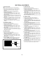
2. REMOVAL OF DVD DECK PARTS

2-1: TRAY (Refer to Fig. 2-1-A)

Set the Tray opened. (Refer to the DISC REMOVAL
METHOD AT NO POWER SUPPLY)
Unlock the 2 supports 

1

 and remove the Tray.

1.

2.

Fig. 2-1-A

Tray

Main Frame Ass'y

1

NOTE

1. In case of the Tray installation, install them as the circled

section of Fig. 2-1-B so that the each markers are met.

2-2: MAIN CHASSIS ASS'Y (Refer to Fig. 2-2-A)

Remove the screw 

1

.

Unlock the 2 supports 

2

.

Remove the Insulator (R) from the Main Frame Ass'y.
Remove the Main Chassis Ass'y.

1.
2.
3.
4.

Fig. 2-2-A

Tray

Main Frame Ass'y

Fig. 2-1-B

Insulator (R)

NOTE

1. Do not disassemble the DVD DECK PARTS except listed

parts here. Minute adjustments are needed if the
disassemble is done. If the repair is needed except listed
parts, replace the DVD MECHA ASS'Y.

1

1

2

Main Frame Ass'y

Main Chassis Ass'y

2

• Screw Torque: 2.0 

±

 0.5kgf•cm

NOTE

1.

2.

In case of the Main Chassis Ass'y, install it from (1) to (4)
in order. (Refer to Fig. 2-2-B)
In case of the Main Chassis Ass'y installation, hook the
wire on the Main Frame Ass'y as shown Fig. 2-2-C.

Fig. 2-2-B

Fig. 2-2-C

(1)

(2)

(3)

(3)

(4)

(3)

Check Lock

(4)

Main Chassis Ass'y

Rack Loading

Main Frame Ass'y (Bottom Side)

Traverse Holder

Summary of Contents for MD14F52

Page 1: ...200605GR MFR S VERSION A The above model is classified as a green product 1 as indicated by the underlined serial number This Service Manual describes replacement parts for the green product When repairing this green product use the part s described in this manual and lead free solder 2 For 1 and 2 see the next page ...

Page 2: ...nt of parts is not only confined to manufacture The same green parts used in manufacture must also be used as replacement parts 2 LEAD FREE SOLDER This product is manufactured using lead free solder as a part of a movement within the consumer products industry at large to be environmentally responsible Lead free solder must be used in the servicing and repair of this product WARNING This product i...

Page 3: ...a ground conductive wrist strap for body Location of the required Marking The rating sheet and the safety caution are on the rear of the unit CERTIFICATION COMPLIES WITH FDA RADIATION PERFORMANCE STANDARDS 21 CFR SUBCHAPTER J CAUTION THIS DIGITAL VIDEO PLAYER EMPLOYS A LASER SYSTEM TO ENSURE PROPER USE OF THIS PRODUCT PLEASE READ THIS SERVICE MANUAL CARE FULLY AND RETAIN FOR FUTURE REFERENCE SHOUL...

Page 4: ...nd turn on the TV Insulation resistance between the cord plug terminals and the eternal exposure metal Note 2 should be more than 1M ohm by using the 500V insulation resistance meter Note 1 If the insulation resistance is less than 1M ohm the inspection repair should be required Note 1 If you have not the 500V insulation resistance meter use a Tester Note 2 External exposure metal Antenna terminal...

Page 5: ...al power company For units intended to operate from battery power or other sources refer to the operating instructions GROUNDING OR POLARIZATION This unit is equipped with a polarized alternating current line plug a plug having one blade wider than the other This plug will fit into the power outlet only one way This is a safety feature If you are unable to insert the plug fully into the outlet try...

Page 6: ... equipment turn off the power and unplug all of the equipment from the wall outlet Failure to do so may cause an electric shock and serious personal injury Read the owner s manual of the other equipment carefully and follow the instructions when making any connections SOUND VOLUME Reduce the volume to the minimum level before you turn on the product Otherwise sudden high volume sound may cause hea...

Page 7: ...A DISCHARGE UNIT NEC SECTION 810 20 ANTENNA LEAD IN WIRE GROUNDING CONDUCTORS NEC SECTION 810 21 GROUND CLAMPS POWER SERVICE GROUNDING ELECTRODE SYSTEM NEC ART 250 PART H GROUND CLAMP ELECTRIC SERVICE EQUIPMENT NEC NATIONAL ELECTRICAL CODE S2898A IMPORTANT SAFEGUARDS CONTINUED ...

Page 8: ...o soldering the Laser may be damaged WHEN REPLACING DVD DECK When removing the DVD Deck When installing the DVD Deck Remove all the soldering on the short circuit position after the connection of Pick Up PCB and DVD PCB connector NOTE Fig 1 Before your operation please read PREPARATION OF SERVICING Use the Lead Free solder Manual soldering conditions Soldering temperature 350 5 C Soldering time Wi...

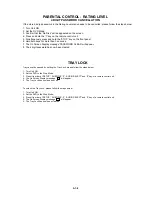
Page 9: ...ELECT and 0 key of a remote control unit The On Screen Display message will appear The Tray Lock has now been cleared 1 2 3 4 5 PARENTAL CONTROL RATING LEVEL 4 DIGIT PASSWORD CANCELLATION If the stored 4 digit password in the Rating Level menu needs to be cancelled please follow the steps below Turn Unit ON Set the DVD Mode Confirm that the No Disc will be appeared on the screen Press and hold the...

Page 10: ... PRINTED CIRCUIT BOARDS DVD AV CRT LOADING MOTOR SW SCHEMATIC DIAGRAMS MPEG MICON DSP MEMORY MOTOR DRIVE AUDIO VIDEO REGULATOR MICON TUNER SOUND AMP IN OUT DEFLECTION CRT POWER CHROMA STEREO LOADING MOTOR SW INTERCONNECTION DIAGRAM WAVEFORMS MECHANICAL EXPLODED VIEWS DVD DECK EXPLODED VIEW MECHANICAL REPLACEMENT PARTS LIST DVD DECK REPLACEMENT PARTS LIST ELECTRICAL REPLACEMENT PARTS LIST A1 1 A1 1...

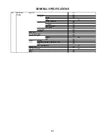
Page 11: ...9 4A A 5 A 1 A I J W W 1 W 84 Intermediate Picture FP 45 75MHz Frequency Sound FS 41 25MHz FP FS 4 50MHz Preset CH No Stereo Dual TV Sound US Stereo Tuner Sound Muting Yes G 4 Signal Video Signal Input Level 1 V p p 75 ohm Output Level S N Ratio Weighted Horizontal Resolution at DVD Mode RGB Signal Output Level Audio Signal Input Level 8 0dBm 50k ohm Output Level Digital Output Level 0 5 V p p 75 ...

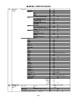
Page 12: ...annel Setup Yes TV CABLE Yes Auto CH Memory Yes Add Delete Yes V chip Setup Yes Language Yes Sleep Timer Yes CH AV LINE DVD Yes Stereo Audio Output Yes Bilingual No SAP Yes Control Volume Yes Level Brightness Contrast Sharpness Color Yes Tint Yes Bass Treble Balance No Caption Text Yes Auto Search Position No Game Yes Mute Yes A3 2 ...

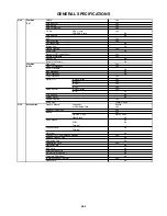
Page 13: ...o disc Yes Reading Yes Play Yes Still Pause Yes Stop Yes Prohibit Mark Yes PBC Yes Step Yes Skip Yes Skip Yes Random Yes CD VIDEO CD JPEG Repeat Yes Slow Yes Slow No Search Yes Search Yes Jump Yes Resume Yes Title No Yes Chapter No Yes Track No Yes Time Yes Sub Title No Yes Angle No Yes Vocal On Off No Audio No Yes Audio Stereo L R Yes Video CD Zoom Yes Marker No Yes Program Play Back Yes CD VIDEO...

Page 14: ...es 9 Yes 0 Yes Play Yes Stop Yes Search Yes Search Yes Closed Caption Skip Yes Quick View CH RTN Skip Yes Slow Yes Slow No Pause Still Step Yes DISPLAY Yes TV DVD Yes Cancel Yes Audio Select Yes Angle Yes Subtitle Yes Top Menu Yes Menu Yes DVD Menu Yes Return Yes CH Up Yes CH Down Yes Vol Down Yes Vol Up Yes Up Set Yes Down Set Yes Left Select Yes Right Select Yes Enter Yes Play Mode Yes Input Sel...

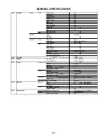
Page 15: ...ayback Yes Digital Out Dolby Digital Yes MPEG Yes PCM Yes DTS Yes Down Mix Out Dolby Digital Yes DTS No 3D Surround No Screen Saver No Closed Caption Yes Audio DAC 192kHz 24bit G 15 Accessories Owner s Manual Language English w Guarantee Card Yes Remote Control Unit Yes Battery Yes UM size x pcs UM 4 x 2 pcs OEM Brand No Rod Antenna No Poles No Terminal Loop Antenna No Terminal U V Mixer No 300 oh...

Page 16: ...No VHF UHF Antenna Input F Type G 17 Set Size Approx W x D x H mm 440x392 5x393 G 18 Weight Net Approx 13 5kg 29 8lbs Gross Approx 15 5kg 34 2lbs G 19 Carton Master Carton No Content Sets Material Dimensions W x D x H mm Description of Origin Gift Box Material Double Brown W Color Photo Label No Dimensions W x D x H mm 550x496x471 Description of Origin Yes Drop Test Natural Dropping At 1 Corner 3 ...

Page 17: ...INS HIGH VOLTAGE BEFORE ATTEMPTING TO REMOVE OR REPAIR ANY PCB UNPLUG THE POWER CORD FROM THE AC SOURCE 1 2 3 Remove the Anode Cap Refer to REMOVAL OF ANODE CAP Disconnect the following connector CP805 Remove the CRT PCB in the direction of arrow CRT PCB Front Cabinet Fig 1 1 Fig 1 2 Front Cabinet Front Cabinet 1 1 2 1 Back Cabinet 3 1 1 4 DVD BLOCK Refer to Fig 1 4 1 2 3 4 5 6 7 8 Remove the 11 s...

Page 18: ...VD PCB DVD DECK Refer to Fig 1 5 NOTE Before your operation please read PREPARATION OF SERVICING Use the Lead Free solder Manual soldering conditions Soldering temperature 350 5 C Soldering time Within 2 seconds Soldering combination Sn 3 0Ag 0 5Cu When Soldering Removing of solder use the drawing equipment over the Pick Up Unit to keep the Flux smoke away from it When installing the DVD Deck remo...

Page 19: ... the Main Frame Ass y Remove the Main Chassis Ass y 1 2 3 4 Fig 2 2 A Tray Main Frame Ass y Fig 2 1 B Insulator R NOTE 1 Do not disassemble the DVD DECK PARTS except listed parts here Minute adjustments are needed if the disassemble is done If the repair is needed except listed parts replace the DVD MECHA ASS Y 1 1 2 Main Frame Ass y Main Chassis Ass y 2 Screw Torque 2 0 0 5kgf cm NOTE 1 2 In case...

Page 20: ...lt Pulley Gear 1 Main Frame Ass y 2 3 LOADING MOTOR PCB ASS Y LOADING BELT Refer to Fig 2 3 A 1 2 3 4 5 Remove the Loading Belt Remove the screw 1 Remove the 2 screws 2 Remove the Loading Motor PCB Ass y Remove the Pulley Gear Fig 2 3 A 2 2 Loading Motor PCB Ass y Screw Torque 2 5 0 3kgf cm Screw 1 Screw Torque 1 0 0 3kgf cm Screw 2 Rack Loading 1 Main Frame Ass y Main Gear Pulley Gear 2 Fig 2 4 A...

Page 21: ... surface for pressing of the insert Feed Motor Motor Gear NOTE 1 2 3 4 When pushing the Rack Feed in the direction of the arrow it should be restored to the original position by the spring force Refer to Fig 2 7 B In case of the Motor Gear installation check if the value of the Fig 2 7 C is correct When installing the wire of the Switch PCB Ass y install it correctly as Fig 2 7 D After the assembl...

Page 22: ...pin FFC When installing the FFC fold it correctly and install it as shown from Fig 2 8 A to Fig 2 8 C 2 8 FFC WIRE HANDLING 1 Do not make the folding lines except the specified positions for the FFC 1 NOTE Fig 2 8 A Proceed the steps 1 through 4 6 pin FFC Fig 2 8 B Printing Surface Reinforcement Plate 55 1mm Fold 1 Printing Surface 10 1mm Fold 3 Printing Surface 60 1mm Fold 4 Printing Surface Prin...

Page 23: ...ip up the sides of the Rubber Cap in the direction of the arrow and remove one side of the support Refer to Fig 3 2 2 GND on the CRT Screwdriver Alligator Clip Support CRT GND on the CRT Rubber Cap CRT Support Fig 3 1 Fig 3 2 3 After one side is removed pull in the opposite direction to remove the other NOTE DISASSEMBLY INSTRUCTIONS INSTALLATION 1 Clean the spot where the cap was located with a sm...

Page 24: ...ompletely Fig 4 2 Blower type IC desoldering machine IC 3 When IC starts moving back and forth easily after desoldering completely pickup the corner of the IC using a tweezers and remove the IC by moving with the IC desoldering machine Refer to Fig 4 3 NOTE Some ICs on the PCB are affixed with glue so be careful not to break or damage the foil of each IC leads or solder lands under the IC when rem...

Page 25: ...eld Wire Refer to Fig 4 7 NOTE Do not absorb the solder to excess Fig 4 7 Soldering Iron IC Braided Shield Wire 4 When bridge soldering between terminals and or the soldering amount are not enough resolder using a Thin tip Soldering Iron Refer to Fig 4 8 Fig 4 8 Thin tip Soldering Iron IC 5 Finally confirm the soldering status on four sides of the IC using a magnifying glass Confirm that no abnorm...

Page 26: ...h VOL DOWN button on the set and Channel button 8 on the remote control for more than 2 seconds After the confirmation of each check sum turn off the power Rom correction data check sum OEC6087A_115 INIT 1773 ROM 20C2 CRT ON 0000 VOL DOWN Minimum 1 2 sec TV mode Initialization of factory TV data NOTE Do not use this for normal servicing If you set factory initialization the memories are reset such...

Page 27: ...ntil Press RIGHT LEFT button to select DATA When DATA is selected it will blink Again step through the DATA using UP DOWN button until required DATA value has been selected Pressing RIGHT LEFT button will take you back to ADDRESS for further selection if necessary Repeat steps 4 to 6 until all data has been checked When satisfied correct DATA has been entered turn POWER off return to STANDBY MODE ...

Page 28: ... on the remote control to end the adjustments 3 4 01 OSD 17 Function Step No Fig 1 2 NO 01 02 03 04 05 06 07 08 09 10 11 12 13 14 15 16 17 18 19 20 21 22 23 24 25 26 27 FUNCTION CNTNA COLCA COLXA COLNA TNTCA SHRPA BRTCD BRTXD BRTND CNTCD CNTXD CNTND COLCE COLXD COLND TNTCD SHRPD BRTCG BRTXG BRTNG CNTCG CNTXG CNTNG TVM PVM LVL SEPAL SEPAH NO 28 29 30 31 32 33 34 35 36 37 38 39 40 41 42 43 44 45 46 ...

Page 29: ... Using the remote control set the brightness and contrast to normal position Activate the adjustment mode display of Fig 1 1 and press the channel button 05 on the remote control to select VSIZ Press the RIGHT LEFT button on the remote control until the SHIFT quantity of the OVER SCAN on upside and downside becomes 10 2 Receive a broadcast and check if the picture is normal 2 8 BRIGHT CENTER 1 2 3...

Page 30: ...d press the channel button 40 on the remote control to select COLCD Press the RIGHT LEFT button on the remote control to set the same the same step numbers as the AV Fig 2 4 2 9 OSD POSITION Activate the adjustment mode display of Fig 1 1 Press the RIGHT LEFT button on the remote control until the difference of A and B becomes minimum Refer to Fig 2 2 1 2 B A Fig 2 2 01 OSD 17 White 0 White 100 Re...

Page 31: ...button 38 on the remote control to select CNTXD Press the RIGHT LEFT button on the remote control to set the same step numbers as the AV Press the INPUT button on the remote control to set to the GAME mode Activate the adjustment mode display of Fig 1 1 and press the channel button 49 on the remote control to select CNTXG Press the RIGHT LEFT button on the remote control to set the same the same s...

Page 32: ...s between the deflection yoke and CRT funnel to fix the deflection yoke Refer to Fig 3 2 b R G B R G B Fig 3 2 a WEDGE WEDGE WEDGE WEDGE POSITION Fig 3 2 b R G B R G B Receive the crosshatch pattern from the color bar generator Combine red and blue of the 3 color crosshatch pattern on the center of the screen by adjusting the pair of 4 pole magnets Combine red blue magenta and green by adjusting t...

Page 33: ...CRT CRT CRT PCB J801 CP802B CP803B TP024 TP023 TU001 J4201 VR3800 CP803A FB401 CP3800 CP401 CP302 CP802A CP8002 CP8001 CP301 J2202 J2203 J2204 J2201 AV PCB CD805 CD803 CD802 CD301 CD302 S3801 S3802 CD2301 CD2001 CP2301 CP2303 CP2302 CP8101 CD4002 CD2302 CD3800 SPEAKER SP351 SPEAKER SP352 VR402 TP022 TP401 R408 CP101 CD8101 ...

Page 34: ...SPDL SPINDLE SLED FOCUS TRACK_PWM TRAY_CLOSE OPEN E A B DVD BLOCK DIAGRAM HA0 A19 HD0 D15 MEMCS0 RD WR SD_A0 A10 SD_D0 D15 16M SDRAM IC4009 M12L16161A 7TG A A REG 3 3V 1 9V IC4003 BA33E00WHFP TR TV BLOCK SSCCLK RDY I O 0 SPDIF DVD RESET AUDIO L AUDIO R ZERO STEREO DAC IC8102 PCM1753DBQR DVD Y DVD C C A B ML MC MD AMCLK ABCLK ALRCLK ASDATA0 D E 1 A 3 3V B 1 8V C 3 8V D 5V E 6V D DRVSB E 2 DVD CDPD ...

Page 35: ... CLOSE PLAY VOL UP VOL DOWN CH UP 28 27 X101 16MHz TV BLOCK DIAGRAM 34 43 33 J2202 FROM DVD BLOCK DVD C DVD Y A AT 5V B P CON 9V C P CON 5V D P CON 12V POWER ON OFF SKIP REW L V 2 2 2 R J2203 J2204 CH DOWN 7 11 J4201 2 SPDIF Q4201 DRIVER DVD_RESET 3 F 9 8 7 E 3 22 8 14 27 15 29 28 32 E 4 SOUND AMP IC353 AN7513 4 2 6 8 24 30 23 21 AUDIO OUT 13 36 37 16 SOUND B 8 5 6 SSCCLK Q4202 Q4204 Q4206 MUTE SW...

Page 36: ... VR3800 B ADJ IC3800 PS2561AL1 1 V W FB401 2 4 2 MOTOR 6V REG IC3001 BA00BC0WT V5 POWER BLOCK DIAGRAM UNREG 3 8V AT 5V SOUND B P CON 9V POWER ON H B POWER FEED BACK MOTOR B 6V 10 P CON 12V DRIVER Q3005 DRIVER Q3002 P ON SW Q3007 DRIVER Q3008 P ON SW Q3003 E 5 E 6 2 1 P CON 5V REG IC3002 KIA278R05PI DRIVER Q3001 P CON 5V P CON 5V DVD ...

Page 37: ...001 R2335 D2303 D2304 D8112 C4100 C4063 C4090 B4009 W854 W826 W824 W843 IC2301 C4089 CD4002 C8106 C8122 D8111 W808 R4050 R4033 C8107 IC4009 R4059 C4106 C4074 C4008 W829 C2309 C4109 R2320 R2310 C8121 CP8101_3 PRINTED CIRCUIT BOARDS DVD TOP SIDE C8108 C8120 B8103 C4099 R4037 R4036 C4072 C4026 C4034 C4035 R4012 R4042 R4018 R4016 C4065 C4080 C4097 C4015 C4052 C4012 C4075 C4014 B4003 C2358 R2323 C2360 ...

Page 38: ...5 C610 C645 C618 C625 C621 C630 X602 D602 D603 D605 C604 C638 C609 C643 W050 C639 C629 W063 L601 C642 W147 L603 R603 C613_1 R602 R612 W198 W060 CP805 C802 D806 D804 D805 CP802B CP803B L801_1 R803 R805 R807 CP806 TP022 TP023 TP024 Q804 Q805 Q806 W813 W852 R3817_1 W871 W873 W872 W880 W879 R434_2 C402 R408 W178 W159 W160 W165 W166 R4281 R4282 W153 W172 W189 W209 W205 W206 W191 W193 W195 W196 W197 W20...

Page 39: ...32 C337 C348 C334 C333 IC902 R910 C929 C934 C937 C939 C950 C951 C933 C935 R908 R913 C938 R126 R109 C110 R120 R114 Q3804 C335 C3016 Q601 R607 R605 R644 C612 C616 R611 R641 C628 R643 R610 R609 C608 R618 C631 C632 IC601 C641 C633 R616 Q602 R619 Q605 R814 R816 R811 R815 R809 R813 C810 C809 C811 R305 R308 R131 I C 1 0 1 IC199_1 R647 R628 Q3003 C3012 R428 R420 Q4205 R4202 Q4204 Q4203 R4201 R117 Q4202 Q4...

Page 40: ...SW1 CD2302 PRINTED CIRCUIT BOARDS F 7 F 8 LOADING MOTOR INSERTED PARTS SOLDER SIDE LOADING MOTOR CHIP MOUNTED PARTS SOLDER SIDE SW SOLDER SIDE D D0 0 RE BLUE OR BL SW2 CD2301 M2602 M2601 ...

Page 41: ...ND P CON 3 3V TRAY_OPEN TRAY_CLOSE HOME HA0 TOUT_SW HA1 TIN_SW HA2 DVD CD HA3 HA15 DRVSB HA4 RF HA5 HA16 DAC_VIDEO_C OPU_A HA6 HA14 DAC_VIDEO_B OPU_B HA7 HA13 DAC_VIDEO_D OPU_C HA8 HA12 OPU_D HA9 OPU_E HA10 HD15 OPU_F HA11 HA11 VC HA12 HD7 SPDL_SENS HA13 SPDL_SENS HA14 HA15 HA10 P H I L DVD CDPD HA16 DVD_LD HD14 HA17 CD_LD HA9 RESET HA18 SPINDLE_PWM HD6 HA19 SLED_PWM HA8 TRACK_PWM HD0 FOCUS_PWM HD...

Page 42: ...14 SD_D15 HD5 HA19 RAMCS0 RAMRAS RAMCAS HD12 SD_BA0 SD_D9 SD_D6 RAMDQM RAMWE HD4 WR RAMCLK SD_D8 SD_D7 RESET HA0 HA1 HD11 HA2 RAMDQM HA3 HA4 HD3 HA5 RAMDQM RAMWE HA6 HA7 HD10 HA19 HA8 RAMCLK RAMCAS HA9 HA10 HD2 HA18 HA11 RAMRAS HA12 RAMCKE HA13 HD9 HA17 HA14 RAMCS0 HA15 HA16 HD1 HA7 HA17 SD_A9 SD_BA0 HA18 HA19 HD8 HA6 SD_A8 SD_A10 HD0 HD1 HD0 HA5 HD2 SD_A7 SD_A0 HD3 HD4 RD HA4 HD5 SD_A6 SD_A1 HD6 ...

Page 43: ...0_1 100 10V KA C2340_1 100 6 3V KA C2343_1 47 6 3V KA Q2305 KTC3875S_Y_RTK VR DVD Q2304 KTC3875S_Y_RTK DVD CD Q2303 KTC3875S_Y_RTK VR DVD W843 OF PRINTING AND SUBJECT TO CHANGE WITHOUT NOTICE NOTE THIS SCHEMATIC DIAGRAM IS THE LATEST AT THE TIME DANS LA NOMENCLATURE DES PIECES N UTILISER QUE CELLS DECRITES DANGEREUSES AN POINT DE VUE SECURITE LES PIECES REPAREES PAR UN ETANT ATTENTION SINCE THESE ...

Page 44: ...E NOTE THIS SCHEMATIC DIAGRAM IS THE LATEST AT THE TIME DURING PLAYBACK MEASURED WITH THE DIGITAL TESTER NOTE THE DC VOLTAGE EACH PART WAS CP8101_3 IMSA 9604S 12F 1 10 11 12 2 3 4 5 6 7 8 9 DAC_C_VIDEO DAC_VIDEO_C DAC_VIDEO_C DAC_VIDEO_B P CON 5V RESET DAC_VIDEO_B DAC_B_VIDEO MC MD ML AMCLK ABCLK ALRCLK ASDATA0 P H I L P H I L DVD H SYS_MUTE GND RESET ZERO R_AUDIO L_AUDIO DAC_B_VIDEO DAC_C_VIDEO D...

Page 45: ... WITH THE DIGITAL TESTER NOTE THE DC VOLTAGE EACH PART WAS R3005 1 8 3W CP8002 IMSA 9604S 12C 1 10 11 12 2 3 4 5 6 7 8 9 IC3002 KIA278R05PI P CON 5V_REG IC 1 2 3 4 IC3001 BA00BC0WT V5 MOTOR 6V_REG IC 1 2 3 4 5 CP8001 A2001WV2 13P 1 10 11 12 13 2 3 4 5 6 7 8 9 S802Y UNREG 5V UNREG 5V POWER_ON_H P CON 5V GND P CON 9V UNREG 12V P CON 12V P CON 5V UNREG 8V GND UNREG 3 8V DVD_Y DVD_C UNREG 8V P CON 5V ...

Page 46: ...E CELLS DECRITES DANGEREUSES AN POINT DE VUE SECURITE LES PIECES REPAREES PAR UN ETANT ATTENTION SINCE THESE PARTS MARKED BY CAUTION DESCRIBED IN PARTS LIST ONLY CRITICAL FOR SAFETY USE ONES ARE SCL SDA I2C_OFF REMOCON KEY_A KEY_B POWER_ON_H TUNER_VIDEO TUNER_AUDIO 30V P CON 5V FSC_OUT POWER_FAIL AFT SCL SDA SDA SCL VIDEO_OUT TUNER_AUDIO SCL SDA REMOCON TUNER_AUDIO OSD_Y OSD_B OSD_G OSD_R POWER_ON...

Page 47: ...2 18K 1 4W R308 10K R305 10K C340 10 50V KA C341 10 50V KA W852 OF PRINTING AND SUBJECT TO CHANGE WITHOUT NOTICE NOTE THIS SCHEMATIC DIAGRAM IS THE LATEST AT THE TIME DANS LA NOMENCLATURE DES PIECES N UTILISER QUE CELLS DECRITES DANGEREUSES AN POINT DE VUE SECURITE LES PIECES REPAREES PAR UN ETANT ATTENTION SINCE THESE PARTS MARKED BY CAUTION DESCRIBED IN PARTS LIST ONLY CRITICAL FOR SAFETY USE ON...

Page 48: ... YK Q4201 KTC3875S_Y_RTK D AUDIO DRIVER Q4204 KTC3875S_Y_RTK MUTE SW Q4203 KTC3875S_Y_RTK MUTE SW W804 W825 W821 W834 W820 OF PRINTING AND SUBJECT TO CHANGE WITHOUT NOTICE NOTE THIS SCHEMATIC DIAGRAM IS THE LATEST AT THE TIME DANS LA NOMENCLATURE DES PIECES N UTILISER QUE CELLS DECRITES DANGEREUSES AN POINT DE VUE SECURITE LES PIECES REPAREES PAR UN ETANT ATTENTION SINCE THESE PARTS MARKED BY CAUT...

Page 49: ... R415 2 7 1 2W R418 2 7 1 2W R414 4 7K 1 4W R422 560 1 2W R411 18K 1 4W R404 56K 1 2W R433 10K 1 4W R406 47K 1 4W R407_1 680 1 4W R460 100 1 4W R445_1 39K 1 4W R453 120K 1 2W R421 560 1 2W R423 10K 1 4W R430 33K 1 2W R403 1K 1 4W R424 3 3K 1 4W R417 560 1 2W R467 1 1 2W R416 27K 1 4W R409 22K 1 4W R410 5 6K 1 4W R405 56K 1 2W R428 10K R420 10K C406 100 35V MHE C405 1 50V YK C401 10 100V YK C431 22...

Page 50: ...K 1 4W Q804 2SC4217 BLUE OUT Q805 2SC4217 GREEN OUT Q806 2SC4217 RED OUT W879 W880 W861 W872 W873 W871 W878 OF PRINTING AND SUBJECT TO CHANGE WITHOUT NOTICE NOTE THIS SCHEMATIC DIAGRAM IS THE LATEST AT THE TIME DANS LA NOMENCLATURE DES PIECES N UTILISER QUE CELLS DECRITES DANGEREUSES AN POINT DE VUE SECURITE LES PIECES REPAREES PAR UN ETANT ATTENTION SINCE THESE PARTS MARKED BY CAUTION DESCRIBED I...

Page 51: ...820 4 7 50V YK C3815 470 200V UP C3823 1000 25V MHE C3805 0 022 B C3816 0 0047 250V KX C3812 0 001 500V B C3807 0 047 100V MMTS C3801 0 33 275V ECQUL C3814 0 0039 500V B C3810 0 001 500V B C3809 0 012 B C3806 0 01 B C3811 0 0015 2KV R C3802 0 01 B C3824 470P 2KV R R3829 100 1 4W R3833 330 1 4W R3826 1 2M 1 2W R3827 1 2M 1 2W R3816 680 1 4W R3818 330 1 4W R3822 1K 1 2W R3803 1 5M 1 2W R3806 2 7M 1 ...

Page 52: ... KTC3875S_Y_RTK SW Q601 KTC3875S_Y_RTK SW W867 W853 W850 W822 W832 W827 W843 OF PRINTING AND SUBJECT TO CHANGE WITHOUT NOTICE NOTE THIS SCHEMATIC DIAGRAM IS THE LATEST AT THE TIME S804Y DVD_Y DVD_C P CON 5V P CON 8V P CON 8V GND P CON 8V PROTECT H_OUT AFC H_CONTROL P CON 5V ACL SYNC_VIDEO P CON 8V V_OUT HD V_RANP_FB VD OSD_B OSD_G OSD_R SW_A_OUT_L OSD_Y SDA FSC_OUT SCL POWER_ON_H DVD_A_OUT_R2 VIDE...

Page 53: ...ATIC DIAGRAM IS THE LATEST AT THE TIME DANS LA NOMENCLATURE DES PIECES N UTILISER QUE CELLS DECRITES DANGEREUSES AN POINT DE VUE SECURITE LES PIECES REPAREES PAR UN ETANT ATTENTION SINCE THESE PARTS MARKED BY CAUTION DESCRIBED IN PARTS LIST ONLY CRITICAL FOR SAFETY USE ONES ARE SCL TUNER_AUDIO SDA JACK_AUDIO_L JACK_AUDIO_R AUDIO_OUT_L AUDIO_OUT_R FRONT_A_IN_L FRONT_A_IN_R P CON 5V GND G 25 G 26 TO...

Page 54: ...MOTOR LOADING MOTOR DED003 PCB610 DED002 PCB640 BCZ3B52 M2603 CD2302 2H052601 M M 5 4 3 2 1 6 5 4 3 2 1 GND SW FEED MOTOR SPINDLE MOTOR SPINDLE MOTOR FEED MOTOR PICK UP INNER LIMIT SWITCH SW2 JCV9B06 M2601 BCZ3B03 M2602 ESE22MH24 CD2301 2H062102 M SINCE THESE PARTS MARKED BY CAUTION DESCRIBED IN PARTS LIST ONLY CRITICAL FOR SAFETY USE ONES ARE DANS LA NOMENCLATURE DES PIECES N UTILISER QUE CELLS D...

Page 55: ...M P CON A5V GND A GND D GND D SPDIF P CON 3 8V P CON 3 8V SSCCLK TX RDY I O 0 RX SSCRXD SSCTXD P CON 6V CCE062 CME066 DME060 J801_1 FB401_1 FBT YELLOW WHITE SWD_VIDEO CD8101 FFC 5 4 3 2 1 5 4 3 2 1 DVD CD VREF MON DVD NC SW VOL DVD GND DVD LD DVD LD CD VOL CD GND CD MON COM RF C B A D F E VCC F F T T DVD CD GND PDIC CRT PCB PCB110 8 OHM 8 OHM F 1 3 4 5 6 7 8 9 CRT SOCKET PCBD20 TM101 COMMAND TRANS...

Page 56: ...c diagram NOTE 23 24 26 27 POWER ON 0 2ms 1 0V POWER ON 0 2ms 1 0V POWER ON 50µs 1 0V POWER ON 20µs 0 5V AUDIO VIDEO CHROMA 6 7 500µs 500mV 500µs 500mV 25 POWER ON 5ms 1 0V MPEG MICON DSP 1 10ns 100mV 2 5ns 20mV 5 5ns 500mV MEMORY MICON TUNER 22 POWER ON 0 2ms 1 0V 10 10µs 200mV 9 10µs 200mV 3 20ns 1 0V 4 200ns 1 0V ...

Page 57: ...10µs 0 5V SOUND AMP 30 31 POWER ON 10µs 2 0V POWER ON 10µs 2 0V 32 POWER ON 10ms 0 5V 33 POWER ON 20µs 0 5V 34 POWER ON 20µs 2 0V IN OUT 35 36 POWER ON 1ms 100mV POWER ON 1ms 100mV 37 DVD PLAY 0 5ms 200mV 38 DVD PLAY 0 5ms 200mV 28 STANDBY 0 5µs 100mV 29 POWER ON 10µs 2 0V STEREO 40 42 POWER ON 1ms 200mV POWER ON 1ms 50mV 41 POWER ON 1ms 200mV ...

Page 58: ...f the corresponding balloon number in the schematic diagram NOTE POWER 48 49 STANDBY 5µs 5 0V STANDBY 5µs 5 0V SOUND AMP 50 1ms 50mV CRT 45 POWER ON 20µs 5 0V DEFLECTION 43 POWER ON 5ms 10 0V 44 POWER ON 20µs 5 0V 51 1ms 50mV 47 46 POWER ON 20µs 50V POWER ON 20µs 50V ...

Page 59: ...DED VIEW 201 201 201 116 201 PCB110 CRT PCB ASS Y 202 202 202 202 102A 102 202 114 102C 102C 102B 206 117 101C 101D 101B 101A 101K 101 A 213 101H 101J 101J 101J 210 210 204 204 101G 101E 101F 210 210 101I 204 101J 101I 204 ...

Page 60: ... 208 MECHANICAL EXPLODED VIEW I1 2 108 208 208 208 208 208 208 208 208 118 208 208 208 208 209 209 209 209 212 212 106 106 PCB130 DVD PCB ASS Y 115 208 208 208 208 111 211 206 206 103 205 205 205 PCBD20 AV PCB ASS Y 105 207 107 109 206 203 A 203 ...

Page 61: ...MECHANICAL EXPLODED VIEW PACKING DIAGRAM I1 3 124 127 128 129 130 BL001 TM101 124 126 125 123 122 123 120 121 ...

Page 62: ...04 612 614 615 613 602 609 611 AA AA AA AA AA AA AA AA AA AA AA Do not replace the parts Because minute adjustments are needed if this condition is disassembled further more If the repair is needed replace the DVD MECHA ASS Y SW2 PCB640 SW PCB ASS Y CD2001 CD2301 M2602 603 601 605 605 606 702 705 703 SW1 PCB610 LOADING MOTOR PCB ASS Y CD2302 701 607 604 705 617 616 618 Cannot supply by a unit 619 ...

Page 63: ...99853 752WSA0488 SHIELD DECK 116 72795687 741WUA0021 SPRING EARTH 117 72783657 726000A136 SHEET CRT SERVICEMAN 118 72795680 8995034000 CORD CLIP UL CO 119 72783197 753WEA0033 SHEET CU 120 72783658 723000D235 SHEET BAR CODE 121 72782852 791WHAA137 LIGHTRON SHEET 122 72795621 791WHAA126 FILM BAG 123 72781016 792WHAA148 PACKAGE BOTTOM 124 72781017 792WHAA149 PACKAGE T0P 125 72783659 793WCDD055 GIFT B...

Page 64: ...98838 92P100092A TRAY 616 72798836 92P100089A RACK FEED 1 617 72798837 92P100090A RACK FEED 2 618 72798849 92P300020A SPRING RACK FEED 619 72795888 800WFAA008 CUSHION C 701 72795782 811022680U SCREW TAP TITE P BIND 2 6 8 CH 702 72795783 814011723U SCREW PAN M1 7 2 3 P3 CH 703 72795784 816112080U SEMS TAP TITE P PAN W10 2 8 CH 704 72795785 814011730U SCREW PAN M1 7 3 P3 CH 705 72796070 811022080U S...

Page 65: ... 2200 UF 10V C3011 72797374 E02LF1222M CE 2200 UF 10V C3801 72794401 P2122B334M CMP 0 33 UF 275V ECQUL C3810 72795629 C0JTB0513K CC 0 001 UF 500V B C3811 72795581 C0PLRR7E3K CC 0 0015 UF 2KV R C3812 72795629 C0JTB0513K CC 0 001 UF 500V B C3815 72795573 E51CGC471M CE 470 UF 200V C3816 72795579 CD39E0MQ3M CC 0 0047UF 250V C3818 72794381 E5EZF3222M CE 2200 UF 25V C3822 72797483 E5EZT2102M CE 1000 UF ...

Page 66: ...1VT001330 DIODE SILICON 1SS133T 77 D3828 72783212 D9WU02R22B DIODE ZENER MTZJ2 2B EIC D3829 72794483 D2WXN49370 DIODE SILICON 1N4937 D3831 72783213 D9WU03R92B DIODE ZENER MTZJ3 9B EIC D4002 72795897 DD7R0S3550 DIODE SILICON 1SS355 TE 17 D4003 72795897 DD7R0S3550 DIODE SILICON 1SS355 TE 17 D4004 72795897 DD7R0S3550 DIODE SILICON 1SS355 TE 17 D4005 72795897 DD7R0S3550 DIODE SILICON 1SS355 TE 17 D400...

Page 67: ...0K COIL 10 UH L801 72796499 021673560K COIL 56 UH L902 72794540 02167F101J COIL 100 UH L3800 72796403 028R140023 COIL DEGAUSS 8R140023 L3801 72798949 029X000131 COIL LINE FILTER SS26V R150162 L4001 72795936 02167F2R2J COIL 2 2 UH L4002 72796088 02AHB9A972 CORE FERRITE W5T29X7 5X19 L4202 72794540 02167F101J COIL 100 UH L8102 72795943 02167F1R0K COIL 1 UH L8103 72795943 02167F1R0K COIL 1 UH T401 727...

Page 68: ...TOR PCB SIDE A2361WV2 2P CD3800 72795554 1209414909 CORD AC BUSH 9414909 CD4002 72783178 06CU2D2202 CORD CONNECTOR CU2D2202 CD8101 72797046 122F0C1602 CORD JUMPER 2F0C1602 CP2301 72783177 069KYOT159 CONNECTOR PCB SIDE LD07T2 24ND 03 CP2302 72799012 069EV53030 CONNECTOR PCB SIDE 00_6232_005_006_800 CP2303 72799013 069EV63030 CONNECTOR PCB SIDE 00_6232_006_006_800 CP3800 72796821 069S420110 CONNECTO...

Page 69: ...TOSHIBA CORPORATION 1 1 SHIBAURA 1 CHOME MINATO KU TOKYO 105 8001 JAPAN ...

Reviews: