SECTION 2
PART REPLACEMENT AND
ADJUSTMENT PROCEDURES
CAUTIONS BEFORE STARTING SERVICING
Electronic parts are susceptible to static electricity and may easily damaged, so do not forget to take a proper grounding
treatment as required.
Many screws are used inside the unit. To prevent missing, dropping, etc. of the screws, always use a magnetized screw-
driver in servicing. Several kinds of screws are used and some of them need special cautions. That is, take care of the
tapping screws securing molded parts and fine pitch screws used to secure metal parts. If they are used improperly, the
screw holes will be easily damaged and the parts can not be fixed.
1. REPLACEMENT OF MECHANICAL PARTS
1-1. Cabinet Replacement
1-1-1. Top Cover
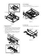
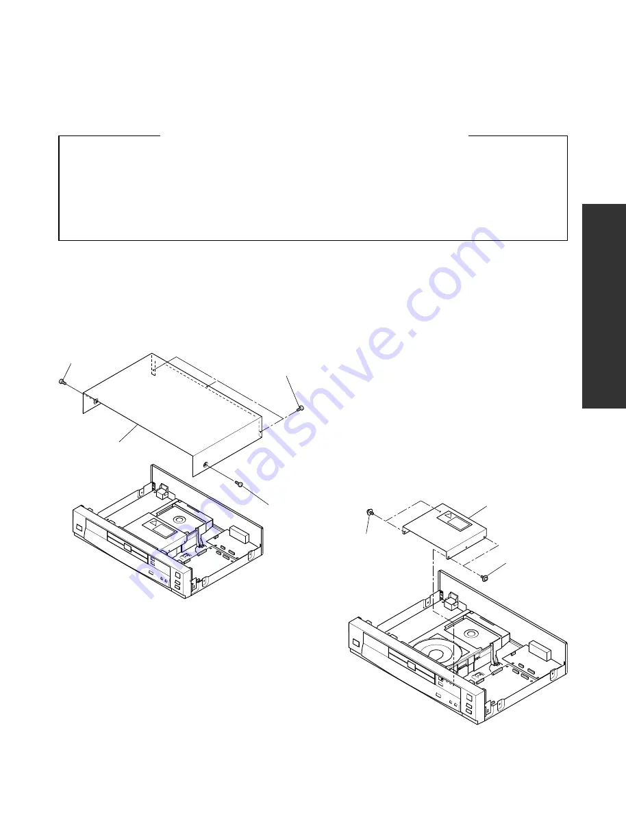
1. Remove five screws (1) and remove the top cover (2).
Fig. 2-1-1
1-1-2. Tray Panel
<Tray Ejection>
1. Remove four screws (1) and remove the mechanism
shield cover (2).
Note:
• When mounting the mechanism shield cover (2),
tighten four screws (1) with the cover lifted as much
as possible, since a little gap is provided between the
cover and the mechanism chassis.
2. Turn the gear (4) clockwise to eject the tray (5). (Refer
to Fig. 2-1-3.)
Fig. 2-1-2
SECTION 2SECTION 2SECTION 2SECTION 2SECTION 2
PPPPPART REPLAART REPLAART REPLAART REPLAART REPLA
CEMENT ANDCEMENT ANDCEMENT ANDCEMENT ANDCEMENT AND
ADJUSTMENT PROCEDURESADJUSTMENT PROCEDURESADJUSTMENT PROCEDURESADJUSTMENT PROCEDURESADJUSTMENT PROCEDURES
Screw (1)
Top cover (2)
Screw (1)
Screws (1)
Screws (1)
Screws (1)
Mechanism
shield cover (2)
Summary of Contents for SD-2050
Page 1: ...DVD VIDEO PLAYER SERVICE MANUAL May 2000 s FILE NO 810 200005 SD 2050 DIGITAL VIDEO ...
Page 5: ...SECTION 1 GENERAL DESCRIPTIONS SECTION 1 GENERAL DESCRIPTIONS 1 OPERATING INSTRUCTIONS ...
Page 51: ...47 Others Memo ...
Page 80: ...4 2 Power Supply Block Diagram Fig 3 4 2 ...
Page 82: ...Fig 3 4 5 4 3 3 Front Display Power Switch Block Diagram ...
Page 84: ...Fig 3 4 7 4 4 2 Logical System Block Diagram ...
Page 85: ...4 5 Output Block Diagram Fig 3 4 8 ...
Page 88: ...10 1 3 4 A B C D E G 2 5 6 7 8 9 F Fig 3 5 3 5 2 Front Display Power Switch Circuit Diagram ...
Page 95: ...Fig 3 5 5 5 3 2 Main Circuit Diagram ...
Page 96: ...5 3 2 Main Circuit Diagram ...
Page 97: ......
Page 98: ......
Page 99: ......
Page 100: ......
Page 101: ......
Page 102: ......
Page 103: ...Fig 3 5 5 ...
Page 105: ...Fig 3 5 6 10 1 3 4 A B C D E G 2 5 6 7 8 9 F 11 H 5 4 Output Circuit Diagram ...
Page 115: ...10 1 3 4 A B C D E G 2 5 6 7 8 9 F Fig 3 6 6 EU01 Main PC Board Top pattern character symbol ...
Page 125: ......


