background image

Summary of Contents for T-Series T3100e

Page 1: ...capacity of 1 Mbyte The hard disk drive HDD has a capacity of 20 Mbytes The floppy disk drive FDD can support 2DD 720 Kbytes and 2HD 1 44 Mbytes floppy disks The universal auto sensing power supply is used for world wide usage The T3100e system unit consists of the following functional modules System board Memory board 3 5 inch floppy disk drive 3 5 inch hard disk drive Plasma display Keyboard Pow...

Page 2: ...6 11 PJ8 9 S1 IS101 102 or Printer PJ 13 External Floppy Disk Drive PJ2 10 System board Memory board Two Serial Devices _ _ _ _ _ _ _ _ _ Option Card 0 0 0 OJ 00 0 0 System Unit PJ2 PJ3 4 PJ5 I IBM PC compatible 0 card 8 Bit PJ14 Cooling Fan PJ7 PJ1 PJ6 PJ3 L _ _ _ _ _ _ _ _ _ _ _ _ _ _ _ _ _ _ 1 3 T 1 0 l HI 1 lQ C Ii rt 1 0 l 0 HI rt T 1 J J rt 1 S C l 1 rt 1 J J T 0 l 1 l HI 1 lQ C Ii 1 I I N I...

Page 3: ...0 x 400 pixel plasma display o A universal auto sensing power supply that can be used world wide provides 5 VDC 12 VDC 5 VDC and 12 VDC power to all the components in the system unit including the option cards For the plasma display the power supply provides the regulated 205 and 5 VDC power The power supply s ventilation fans are driven by 12 VDC o A lithium battery that keeps the date and time e...

Page 4: ...i80286 12 A23 17 23 1 1 0 A23 11 D I GA DMAl A23 11 PJ3 01 01 Ir SAl0 o 10 PJ4 501 0 d RAM 07 0 60PIN COMMAND 82PIN TRANS 1 1 TRANS 74H08 1 1 LS244 12MU d RAM M44256 X8 M81100 X18 I 11MB MD7 U OPTION hj 1 Q C 11 I f l I W Ul r 0 Ul rt r I 0 f 0 X 0 1 Q 11 13 0 H1 rt r I Ul I Ul rt I 3 0 0 11 0 W en en 8 ttl hj 1 f I Z o D m o I o f l o ...

Page 5: ...IO controls the RS232C port o Variable frequency oscillator VFO MB4108A The VFO chip is used for FDD control logic o Two super integration SI JC810 M5M82C800 SI JC810 includes the FDC TC8565 SIO TC8570 and PIT 82C54 SI M5M82C800 includes the two DMACs 82C37 two PICs 82C59 and one PIT 82C54 o Gate arrays The following gate arrays are used in the system board See the T3100e GATE ARRAY SPECIFICATION ...

Page 6: ...42 o Memory Random access memory RAM 1 Mbyte Read only memory ROM 64 Kbytes system BIOS o Gate array The following gate array is used in the memory board See the T3100e GATE ARRAY SPECIFICATION MANUAL for more information EMS controller gate array EMS2 GA 100 pin 1 6 ...

Page 7: ... 1 1 Figure 1 4 3 5 inch FDD Table 1 1 3 5 inch FDD specifications Item Specifications 2 Mbvte mode 1 Mbvte mode Storage Capacity Kbytes Unformatted 2 000 1 000 Formatted 1 440 720 No of Heads 2 2 No of Cylinders 80 80 Access Time ms 1 Track Access 3 3 Average 94 94 Head Settlinq Time 15 15 Recording Density 17434 8717 bit per inch MAX Data Transfer Rate 500 250 Kbytes per second Rotational Speed ...

Page 8: ...with non removable 3 5 inch magnetic disks and mini winchester type magnetic heads The HDD has three jumper straps which are located on the hard disk controller HDC board The HDD is shown in figure 1 5 and its specifications are described in table 1 2 The jumper straps status are shown in table 1 3 Figure 1 5 3 5 inch HDD 1 8 ...

Page 9: ... 34 33 8 27 50 3 575 1 25 4 I 0 3575RPM Typical 5 I Maximum 10 I 0 RPM READY Typical 7 I Maximum 15 I Stop Time s Typical 5 I Maximum 10 M M IInterleave CP3022 3 42 8 1 2 2 1 047 1 400 20 480 41 40 8 25 50 3 557 1 5 M 4 5 M 5 10 7 15 5 10 1 1 1 1 1____________________________ C P 3 0 2 4 1 ______________ IRecording Method 2 7 RLL code 1 ________________________________L __ R u n L e n g t h L i m ...

Page 10: ...rd keys 10 function keys 17 control keys and Fn key The keyboard is a key matrix with one of the 82 keys at each vertex The keyboard is connected to the keyboard controller on the memory board through a 22 pin flat cable The keyboard layout is shown in figure 1 6 Replace key No 3 4 40 41 Figure 1 6 Keyboard 1 10 ...

Page 11: ...isplay is shown in figure 1 7 Figure 1 7 Plasma display Table 1 4 Plasma display specifications Item Specifications No of Dots dots 640 x400 Dot Dimension mm o 16 W x 0 24 H Dot Pitch mm 0 33 W x 0 36 H DisPlav Area mm 192 W x 144 H Contrast more than 1 11 approx 1 13 Color Neon Oranqe Power Requirement Anode Logic E1 5 0 5 V 10 rnA min 400 rnA max Cathode Driver E2 205 5 V 3 rnA min 160 rnA max C...

Page 12: ... 5 inch hard disk drive 5 Plasma display 6 Option boards 7 Cooling fans The above 2 through 4 6 and one of cooling fans receive the power via the system board The power supply unit includes an input line filter line fuse cooling fan power conversion circuitry and connectors Input ratings are 85 to 138 VAC or 170 to 276 VAC less than 130 W when input rating is 115 VAC 60 Hz The power supply unit is...

Page 13: ...tput rating Function DC Max Requration voltaae current tolerance SYstem Board 5 V 5 6 A 5 System Board Coolina Fan 12 V 1 1 A 5 System Board 5 V 300 rnA 5 System Board 12 V 300 rnA 5 Plasma Displav 5 V 60 rnA 10 Plasma Displav 205 V 105 rnA 5V 1 13 ...

Page 14: ...File No 960 010 1 14 ...

Page 15: ...nostics disk 2 Phillips head screwdriver 3 Blade head screwdriver 4 Tweezers 5 2DD and 2HD formatted work disk for FDD testing 6 Cleaning disk kit for FDD testing 7 Multimeter 8 Printer port LED The problem isolation flowchart described in section 2 2 can be used to determine which isolation procedures are necessary to isolate a T3100e problem 2 2 PROBLEM ISOLATION FLOWCHART The flowchart in figur...

Page 16: ...KB message proceed from 64KB to 1024KB Yes IS the C display on the screen yes No Perform power suppl problem isolation procedure in part 2 3 Yes Perform system memory board proble isolation procedures in part 2 4 No Perform display problem isolation procedures in part 2 8 No Perform system memory board problem isolation procedures in part 2 4 No Perform HDD problem isolation procedures in part 2 6...

Page 17: ...n proce ures as indicat d below Figure 2 1 Problem isolation flowchart continued 1 If an error is detected on the system test memory test display test or real timer test perform the system board isolation procedures in section 2 4 2 If an error is detected on the hard disk test perform the HDD problem isolation procedures in section 2 6 3 If an error is detected on the keyboard test perform the ke...

Page 18: ...fter power off to discharge the electricity This section describes how to determine whether or not the power supply unit is defective Start with PROCEDURE 1 and continue with other procedures as instructed The procedures described in this section are PROCEDURE 1 Power Indicator Check PROCEDURE 2 Connector Check PROCEDURE 3 Output Voltage Check PROCEDURE 4 Power Supply Unit Replacement 2 4 ...

Page 19: ...r cord connection One end of the AC power cord should be inserted the standard AC wall outlet and the other end should be connected to the AC IN jack on the back of the system unit If OK replace the AC power cord After replacing the AC power cord if the indicator lights the original cord was probably defective If the indicator still doesn t light go to PROCEDURE 2 2 5 ...

Page 20: ...en unplug the AC power cord 2 Remove the top cover Refer to section 4 8 3 Remove the power supply unit Refer to section 4 9 4 If the power supply connector PJ7 on the system board is connected properly go to PROCEDURE 3 If it is not connected properly reconnect it 2 6 ...

Page 21: ...2 1 the power supply unit is normal but the system board is probably defective Go to the system board isolation procedures in section 2 4 4 If the voltages are still not within the range of values given in table 2 1 go to PROCEDURE 4 Table 2 1 Power supply unit output voltages Pin number Voltage Vdc Connector lead lead Normal Min Max 1 2 5 6 12 11 4 12 6 For 3 2 5 6 12 12 6 11 4 system board 4 2 5...

Page 22: ...ord 2 Replace the power supply unit Refer to section 4 9 3 If normal operation is restored after replacing the power supply unit the original power supply unit was probably defective 4 If normal operation is not restored another FRU is probably defective The defective unit must be isolated and replaced 2 8 ...

Page 23: ...ppy disk in the FDD may result in loss of data This section describes how to determine whether or not the system board is defective Start with PROCEDURE 1 and continue with other procedures as instructed The procedures described in this section are PROCEDURE 1 Message Check PROCEDURE 2 Printer Port LED Check PROCEDURE 3 Test Program Execution PROCEDURE 4 System Board Replacement 2 9 ...

Page 24: ... in CMOS Bad check sum Check system Then press Fl key Error in CMOS Bad configuration Check system Then press Fl key Error in CMOS Bad memory size Check system Then press Fl key Error in CMOS Bad time function Check system Then press Fl key 4 If the following message is displayed on the screen turn off the power Wait 5 seconds or more then turn on the power If the following message is displayed ag...

Page 25: ...channel 0 error DMA channel 1 error DMA page register error Memory refresh error 1st 64KB memory error Error interrupt controller 1 Error interrupt controller 2 VRAM error Memory verify error at X X found X expanded X Memory parity error at X X found X expected X Error interrupt and stuck NMI Error interrupts and stuck NMI Error interrupts and stuck NMI Error protect mode Error sizing expansion me...

Page 26: ...imal value 5 If the final LED status matches any of the error code values in the table 2 3 go to PROCEDURE 4 6 If the final LED status is 33B go to PROCEDURE 3 Status OOH 01H 02H 03H 04H 05H 06H 07H OSH 09H OAR OBH OCH ODH OEH OFH 10H Table 2 2 Printer port LED normal status Error messaae Shutdown process and video initialization CPU test 1 KBC test 1 KBC test 2 KBC test 3 KBC test 4 LSI initializ...

Page 27: ...MOS Battery test CMOS chechsum test Reserved Keyboard initialization 1 VRAM test Video I O initialization System memory size set System memory size check System memory and extra memory test PIC test NMI and parity test Interrupt process test Protect mode test Extended memory size check Extended memory test Protect mode exception processing test Reserved CRT type check PIT interrupt check Hardware ...

Page 28: ... controller 1 Error interrupt controller 2 VRAM error Memory verify error at X X found X expanded X Error interrupt and stuck NMI Error interrupts and stuck NMI Error interrupts and stuck NMI Error protect mode Error sizing expansion memory Memory verify error at X X X found X expected X Memory verify error at X X X found X expected Error processor exceptional interrupts Refresh timing error Error...

Page 29: ...e system test memory test Printer test ASYNC test or real timer test go to PROCEDURE 4 3 If an error is detected during the floppy disk test go to FDD problem isolation procedures in section 2 5 4 If an error is detected during the hard disk test go to HDD problem isolation procedures in section 2 6 5 If an error is detected during the keyboard test go to keyboard problem isolation procedures in s...

Page 30: ... section 4 16 2 If normal operation is restored after replacing the system board the original system board is probably defective 3 If normal operation is not restored another FRU is probably defective The defective unit must be isolated by the test and diagnostics program and replaced 2 16 ...

Page 31: ...rive is defective Start with PROCEDURE 1 and continue with other procedures as instructed The procedures described in this section are PROCEDURE 1 Test and Diagnostics Program Loading Check PROCEDURE 2 Message Check PROCEDURE 3 Head Cleaning PROCEDURE 4 FDD Test Execution PROCEDURE 5 FDD Connector Check PROCEDURE 6 New FDD Connection 2 17 ...

Page 32: ...ing Check 1 Turn off the power 2 Insert the diagnostics disk into the FDD 3 Turn on the power 4 If loading starts normally go to PROCEDURE 3 See section 3 2 to determine if loading has started normally 5 If loading has not started normally go to PROCEDURE 2 2 18 ...

Page 33: ...in drive Press any key when ready 2 If message a is displayed check that the A B PRT switch is set to PRT If it is not set to PRT set it to PRT If it is set to PRT go to PROCEDURE 5 3 If message b or c is displayed the contents of the floppy disk is damaged or a disk other than the diagnostics disk has been inserted into the FDD Insert a new diagnostics disk into the FDD If loading completes go to...

Page 34: ...ead Cleaning 1 Turn off the power 2 Insert the cleaning disk into the FDD 3 Turn on the power 4 If normal operation is restored after cleaning the head go to PROCEDURE 4 5 If normal operation is not restored go to PROCEDURE 5 2 20 ...

Page 35: ...l be displayed The error codes are described in table 2 4 Go to PROCEDURE 6 3 If no error is generated the FDD is normal Table 2 4 FDD error code Code Status 01 Bad Command 02 Address Mark Not Found 03 Write Protected 04 Record Not Found 06 Media Removed 08 DMA Overrun Error 09 DMA Boundary Error 10 CRC Error 20 FDC Error 40 Seek Error 60 FDD Not Drive 80 Time Out Error EE Write Buffer Error 2 21 ...

Page 36: ...g the AC power cord 2 Remove the top cover Refer to section 4 8 3 Check that the FDD connection PJ8 is secure 4 If the FDD cable is securely connected to the system board go to PROCEDURE 6 5 If the FDD cable is not securely connected to the system board secure the connection 2 22 ...

Page 37: ...installing the new FDD Then connect all of the FRUs removed during FDD removal to their corresponding connectors without installing the FRUs 4 Turn on the power 5 If normal operation is restored the original FDD is probably defective Reassemble the system 6 If normal operation is not restored the system board is probably defective Refer to section 2 4 2 23 ...

Page 38: ...ective Start with PROCEDURE 1 and continue with other procedures as instructed The procedures described in this section are PROCEDURE 1 HDD Indicator Check PROCEDURE 2 Message Check PROCEDURE 3 Format Execution PROCEDURE 4 Hard Disk Test Execution PROCEDURE 5 Connector Check PROCEDURE 6 HDD Jumper Straps Check PROCEDURE 7 New HDD Connection 2 24 ...

Page 39: ... FDD take it out 3 Wait 5 seconds or more after turning off the power then turn on the power 960 010 4 If the HOD indicator blinks briefly then goes out go to PROCEDURE 2 If the HOD indicator continues blinking go to PROCEDURE 4 5 If the HOD indicator does not light at all go to PROCEDURE 5 2 25 ...

Page 40: ...stem is loaded normally go to PROCEDURE 4 2 If one of the following message is displayed on the screen go to PROCEDURE 3 HOD Load error or Bad system disk Insert system disk in drive Press any key when ready Check system disk in drive Press any key when ready 2 26 ...

Page 41: ...e MS DOS Manual for details 1 Remove the diagnostics disk from the FDD then insert the MS DOS system disk in 2 Make partition of the hard disk by entering the FDISK command See the MS DOS Manual for details 3 Format the hard disk by entering the FORMAT command See the MS DOS Manual for details At this time use S switch to transfer the system program 4 If normal operation is restored the HDD is nor...

Page 42: ...the hard disk test an error code and status will be displayed go to PROCEDURE 6 The error codes are described in table 2 5 4 If no error is generated the HDD is normal Enter the MS DOS FDISK command to make partition of the hard disk Then enter the MS DOS FORMAT command See the MS DOS Manual for details Code 01 02 04 05 07 09 OA OB 10 11 20 40 80 AA BB CC EO Fa Table 2 5 HDD error code Status Bad ...

Page 43: ...ug the AC power cord 2 Remove the top cover Refer to section 4 8 3 Check that the HDC signal cable PJ6 and HDD power cable PJ11 are secure 4 If both cables are securely connected to the system board go to PROCEDURE 6 5 If the cables are not securely connected secure them 2 29 ...

Page 44: ...e 2 6 3 If the jumper straps are set correctly go to PROCEDURE 7 4 If the jumper straps are not set correctly set them correctly Table 2 6 HDD jumper straps functions 20 Mbyte CP3022 20 Mbyte CP3024 or 40 Mbyte ISignall Status ISignall Status I E5 I Short HSP Open I E6 I Open C D Short I E7 I Short DHP Open ACT Short 20 Mbyte CP3022 20 Mbte CP3024 or 40 Mbyte Figure 2 2 HDD jumper straps 2 30 ...

Page 45: ...D to the system board without installing the HDD Then connect all the FRUs removed during HDD removal without installing the FRUs 4 If normal operation is restored the original HDD is probably defective Reassemble the system 5 If normal operation is not restored the system board is probably defective Refer to section 2 4 2 31 ...

Page 46: ...ermine whether or not the keyboard is defective Start with PROCEDURE 1 and continue with other procedures as instructed The procedures described in this section are PROCEDURE 1 Input Check PROCEDURE 2 Keyboard Test Execution PROCEDURE 3 Connector Check PROCEDURE 4 New Keyboard Connection 2 32 ...

Page 47: ...mat Such operation may erase your important program or data If the character you press appears on the screen press Enter Go to PROCEDURE 2 4 If the character does not appear on the screen go to PROCEDURE 3 Toshiba Personal Computer MS DOS Version X XX RXXXXX C Copyright Toshiba C Copyright Microsoft Current date is XXX X XX 19XX Enter new date mm dd yy Current time is X XX XX XX Enter new time COM...

Page 48: ...cs disk into the FDD and load the test and diagnostics program Refer to section 3 2 Run the keyboard test as indicated on the diagnostic test menu 3 If an error is detected during the test go to PROCEDURE 3 4 If no error is detected during the test the keyboard is normal 2 34 ...

Page 49: ...disconnect the AC power cord 2 Lift up the top cover Refer to section 4 8 3 Lift up the keyboard and check that the keyboard cable PJ3 is securely connected to the system board If it is securely connected go to PROCEDURE 4 4 If it is not securely connected secure it 2 35 ...

Page 50: ...Refer to section 4 2 3 Connect a new keyboard to the system board without installing it 4 If normal operation is restored after connecting the new keyboard the original keyboard is probably defective Install the new keyboard 5 If normal operation is not restored the system board is probably defective Refer to section 2 4 2 36 ...

Page 51: ...ermine whether or not the PLASMA DISPLAY is defective Start with PROCEDURE 1 and continue with other procedures as instructed The procedures described in this section are PROCEDURE 1 Display Check PROCEDURE 2 Display Test Execution PROCEDURE 3 PDP Connector Check PROCEDURE 4 New PDP Connection 2 37 ...

Page 52: ...splayed on the upper left hand corner of the screen 3 4 MEMORY TEST XXXXKB If the above message appears go to PROCEDURE 2 If the above message does not appear a Check that CRT indicator is light If CRT indicator is light hold the Fn key then press the Home key After performing a reperform steps 1 and 2 If the message in step 2 still fails to appear go to PROCEDURE 3 2 38 ...

Page 53: ...diagnostics disk into the FDD and run the display test as indicated on the diagnostic test menu 2 If an error is detected during the display test the system board is probably defective Refer to section 2 4 3 If no error is generated the plasma display is normal 2 39 ...

Page 54: ...urn off the power then unplug the AC power cord 2 Remove the PDP without disconnecting the cables Refer to section 4 5 and check that the cables are securely connected to the plasma display board Refer to figure 2 3 3 If the cable is securely connected go to PROCEDURE 4 4 If the cable is not securely connected secure it Figure 2 3 PDP connector check 2 40 ...

Page 55: ...a new PDP without installing it 2 If normal operation is restored after connecting the new PDP the original PDP is probably defective Reassemble the system 3 If normal operation is not restored the system board is probably defective Refer to section 2 4 2 41 ...

Page 56: ...File No 960 010 2 42 ...

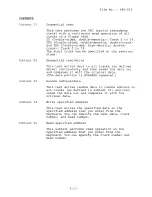
Page 57: ... The test program module is composed of 11 tests 1 SYSTEM TEST 2 MEMORY TEST 3 KEYBOARD TEST 4 DISPLAY TEST 5 FLOPPY DISK TEST 6 PRINTER TEST 7 ASYNC TEST 8 HARD DISK TEST 9 REAL TIMER TEST 10 NDP TEST 11 EXPANSION TEST The following items are necessary for carrying out the test and diagnostic programs 1 T3100e diagnostics disk 2 MS DOS system disk 3 2DD and 2HD formatted work disks For FDD test 4...

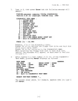
Page 58: ...A Corp 1988 DIAGNOSTICS MENU 1 DIAGNOSTIC TEST 2 HARD DISK FORMAT 3 SEEK TO LANDING ZONE HDD 4 HEAD CLEANING 5 LOG UTILITIES 6 RUNNING TEST 7 FDD UTILITIES 8 SYSTEM CONFIGURATION 9 EXIT TO MS DOS o SETUP PRESS 0 9 KEY Detailed explanations of the service programs and the operations are given in section 3 17 to 3 24 NOTE 1 2 To stop the test program During keyboard operation press Ctrl C While runn...

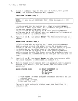
Page 59: ...ostic tests Number 88 is for setting the floppy disk drive and hard disk drive error retry count Number 99 is for returning to the DIAGNOSTICS MENU When selecting the floppy disk test or hard disk test special sub messages will appear as described in sections 3 8 and 3 11 4 After typing in a test number 1 to 11 of the DIAGNOSTIC TEST MENU pressing Enter displays as follows TEST NAME SUB TEST XX PA...

Page 60: ... Enter When an error occurs the error status is displayed and execution of the test program stops and the operation guide is displayed on the right side of the display screen If you select NO by typing in 2 then pressing Enter When an error occurs the error status is displayed then the error counter is incremented by one and you can continue the test 7 Type in 1 or 2 then press Enter and the test ...

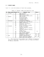
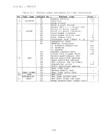
Page 61: ...ssed key display 02 Pressed key code display 01 VRAM read write 1 02 Character attributes 03 Character set 04 80 25 Character display DISPLAY 05 Graphics display color set 0 1 06 640 200 Graphics display mode 6 07 640 400 Graphics display mode 74 08 Display page 14 09 H pattern display 10 LED Font chanqe 01 Sequential read 50 65 02 Sequential read write 80 130 FDD 03 Random address data 10 10 04 W...

Page 62: ...st 60 08 Interrupt test IR04 3 5 2 01 Sequential read 225 02 Address uniqueness 1 Forward sequential 230 2 Reverse 270 3 Random 130 03 Random address data 14 04 Cross talk peak shift 225 05 Write read compare CE 8 HDD 06 Write specified address 07 Read specified address 08 ECC circuit CE cylinder 5 09 Sequential write 115 10 W R C specified address 01 Real time test 02 Backup memory test 1 9 REAL ...

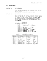
Page 63: ...the hardware status bits If you want to return to the SYSTEM TEST menu press Enter 76543210 H W status 10101100 Bit7 Display mode Plasma Bit6 CPU clock 12MHZ Bit5 Bit4 2MB FDD 2MB Bit3 Internal FDDs 1 Bit2 Drive A B Normal Bitl External FDD OFF BitO Internal FDD 2HD type Table 3 2 Hardware status bit Items H W status 1 0 Bit7 Display mode Plasma CRT Bit6 CPU clock 6MHz 12MHz BitS Reserved Bit4 2MD...

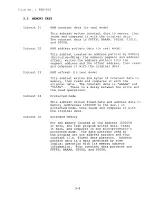
Page 64: ... bytes of constant data to memory then reads and compares it with the original data The constant data is AAAAH and 5555H There is a delay between the write and the read operations Protected mode This subtest writes fixed data and address data to memory addresses 100000H to the max in protected mode then reads and compares it with the original data Extended memory For the memory located at the addr...

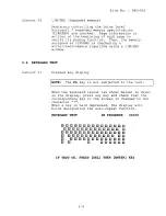
Page 65: ...OTE The Fn key is not subjected to the test When the keyboard layout as shown below is drawn on the display press any key and check that the corresponding key on the screen is changed to the character When a key is held depressed the display will blink designating the auto repeat function KEYBOARD TEST IN PROGRESS fJEJf1JfillBl3fillEll3fillrlJiIfmt1lmJ rn liJ EI IE lID EI IE EI rn lID fID fill ill...

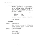
Page 66: ...key top names are shown in APPENDIX E KEYBOARD TEST Scan code Character code Keytop IN PROGRESS XX XX XXXX Ins Lock Alt Caps Lock Ctrl Num Lock Left Shift PRESS Enter KEY 30200 Scroll Lock Right Shift 3 7 DISPLAY TEST Subtest 01 Subtest 02 VRAM read write This subtest writes constant data FFFFH AAAAH 5555H OOOOH and address data to video RAM 256 Kbytes then reads the data written and compares it w...

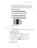
Page 67: ...PLAY I I I I I I I I I I I I I I I I NEXT LINE SHOWS REVERSE DISPLAY NEXT LINE SHOWS BLINKING DISPLAY BBBBBBBBBBBBBBBBBBBBBBBBBBBBBBB PRESS ENTER KEY Character set BLUE RED MAGENTA GREEN CYAN YELLOW WHITE In this subtest the character set of its code OOH to FFH is displayed in the 40 x 25 character mode as shown below CHARACTER SET IN 40X25 j 0123456789 ABCDEFGHI JKLMl lCI P RSTUVWXYZ 1 _ abcdefgh...

Page 68: ...klmnopqrstu 1 0123456789 ABCDEFGHIJKLMNOPQRSTUVWXYZ J _ abcdetghljklmnopqrstuv 10123456789 ABCDEFGHIJKLMNOPQRSTtJVWXYZ _ abcdetghljklmnopqrstuvw 10123456789 ABCDEFGHIJKLMNOPQRSTUVWXYZ J _ abcdetghjjklmnopqrstuvwx 10123456789 ABCDEFGHIJKLMNOPQRSTtJVWXYZ J _ abcdetghljklmnopqrstuvwxy 0123456789 i ABCDEFGHIJKLMNOPQRSTUVWXYZ j _ abcdetghljklmnopqrstuvwxyz 10123456789 ABCDEFGHIJKLMNOPQRSTUVWXYZ j _ abc...

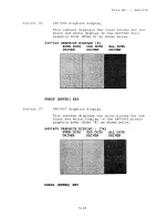
Page 69: ...e Mode 6 as shown below 640 200 GRAPHICS DISPLAY 6 EVEN DOTS ODD DOTS DRIVEN DRIVEN PRESS ENTER KEY 640 400 Graphics display ALL DOTS DRIVEN This subtest displays the color blocks for the black and white display in the 640 400 pixels graphics mode Mode 74 as shown below 640 400 GRAPHICS DISPLAY 74 EVEN DOTS ODD DOTS ALL DOTS DRIVEN DRIVEN DRIVEN PRESS ENTER KEY 3 13 ...

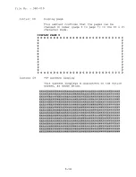
Page 70: ...HHHHHHHHHHHHHHHHHHHHHHHHHHHHHHHHHHHHHHHHHHHHHHH HHHHHHHHHHHHHHHHHHHHHHHHHHHHHHHHHHHHHHHHHHHHHHHHHH HHHHHHHHHHHHHHHHHHHHHHHHHHHHHHHHHHHHHHHHHHHHHHHHHH HHHHHHHHHHHHHHHHHHHHHHHHHHHHHHHHHHHHHHHHHHHHHHHHHH HHHHHHHHHHHHHHHHHHHHHHHHHHHHHHHHHHHHHHHHHHHHHHHHHH HHHHHHHHHHHHHHHHHHHHHHHHHHHHHHHHHHHHHHHHHHHHHHHHHH HHHHHHHHHHHHHHHHHHHHHHHHHHHHHHHHHHHHHHHHHHHHHHHHHH HHHHHHHHHHHHHHHHHHHHHHHHHHHHHHHHHHHHHHHHHHHHHH...

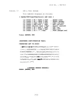
Page 71: ...e key 8 Press Fn key Press ENTER KEY HARDWARE CONFIGURATION TEST CHARACTER SET IN 40X25 Speed red Speed green Caps on off Num on off Scroll on off CRT on CRT off FONT change test 0123456789 ABCDEFGHIJKLMl J PI mSTUVWXYZ 1 _ abcdefghijklrnnopqrstl l o T yz 6 Uea 3 aa eeEn ll AAE A 60oililY TJI f Ptf i6i if iN2 QGr lUSl81 I i1 I 1I J JJ j 1 U f F I l rF irIHfL liT II lJ L rrrlf l r I JIIo I31TILGlJT...

Page 72: ...of the floppy disk to be tested then press the Enter The following message will appear Test start track Enter O dd OO 79 4 You can select the start track number of the floppy disk test When pressing the Enter only the start track number will be zero If you desire select the start track number Then the subtest menu of the floppy disk test will appear 5 During the floppy disk test the message shown ...

Page 73: ...all tracks as defined above continuously and then reads the data out and compares it with the original data The data pattern is B5ADADH repeated Random address data This test writes random data to random address on all tracks as defined in subtest 01 and then reads the data out and compares it with the original data Write specified address This test writes the specified data on the specified addre...

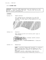
Page 74: ...WXYZ J _ a c e hi jlc lm lopc s 1 0123456789 A3C E GH _ OPQRSTUVWXYZ _ abcce ghijlc lmnopq stu 0123456789 ABCDE GHIJXLMNOPQRSTUVWXYZ 1 _ abccetgh jkl opqrstuv 0123456789 FGH JKLMNOPQRSTUVWXYZ _ abcde ghijk opqrs uv 01234 r OPQRSTUVWXYZ _ abc e l jlc nopqrs 01 P STUVWXYZ _ abcde ghijkl opqrs 0 vwxYZ _ abedetghijlclmnopqr r r _ abedefghijlclmn r fn i 11_ Function This subtest prints out various prin...

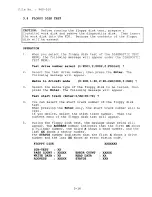
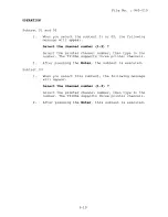
Page 75: ... then type in the number The T3100e supports three printer channels 2 After pressing the Enter the subtest is executed Subtest 03 1 When you select this subtest the following message will appear Select the channel number 1 3 Select the printer channel number then type in the number The T3100e supports three printer channels 2 After pressing the Enter this subtest is executed 3 19 ...

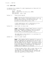
Page 76: ...annel 1 and 2 to execute this test The wiring diagram of the RS 232 C direct cable is described in part 3 25 The same test as the subtest 01 is performed for the channel 1 2 Point to point send NOTE This subtest must be executed in condition that two machines are connected with the RS 232 C direct cable and one side should be set as send and the other set as receive The wiring diagram of the RS 23...

Page 77: ...ich are connected to the PBX Private Branch Exchange One side is set as send and the other set as receive When both sides are ready you can start the test In this subtest data are sent from the send side to the receive side through the PBX This subtest is used to check whether data transmission through a telephone line is done properly or not Dial tester test NOTE To execute this subtest a dial te...

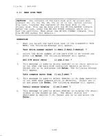
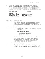
Page 78: ...HDD1 2 2 Select the drive number of the hard disk to be tested and press the Enter The following message will appear HDC F W error retry 1 yes 2 no 3 This message is used to select whether to do retry operation or not when the hard disk controller detects an error Select yes or no and press the Enter The following message will appear Data compare error dump 1 no 2 yes 4 This message is used to sel...

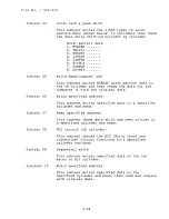
Page 79: ...3 Sequential read This subtest performs forward reading of contents from track 0 to Max track and then performs reverse reading of the contents from Max track to track O Address uniqueness 1 Selecting this subtest the following message will appear Read sequential select 1 Forward sequential 2 Reverse sequential 3 Random 2 Select one of the above and press the Enter This subtest writes the address ...

Page 80: ...cylinder and then reads the data out and compares it with the original data Write specified address This subtest writes specified data to a specified cylinder and head Read specified address This subtest reads data which has been written to a specified cylinder and head ECC circuit CE cylinder This subtest checks the ECC Error check and correction circuit functions to a specified cylinder and head...

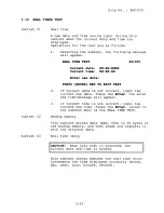
Page 81: ... 2 If current date is not correct input the current new date Press the Enter the enter new time message will appear 3 If current time is not correct input the current new time Press the Enter return to the subtest menu of the REAL TIME TEST Backup memory This subtest writes data AAH 55H to 50 bytes of the backup memory and then reads and compares it with the original data Real time carry CAUTION W...

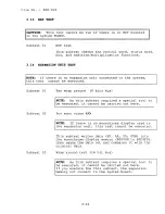
Page 82: ...und 8 bits bus NOTE As this subtest required a special tool to be executed it cannot be carried out here Box mono video RAM NOTE If there is no monochrome display card in the expansion unit this test cannot be executed This subtest writes data FF AA 55 OOH into the monochrome display memory BOOOOH to BOF9FH then reads the data out and compares it with the original data Wrap around test 16 bit bus ...

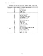
Page 83: ... Bad Command 02 Address Mark Not Found 03 Write Protected 04 Record Not Found 06 Media Removed 08 DMA Overrun Error 09 DMA Boundary Error 10 CRC Error 20 FDC Error 40 Seek Error 60 FDD Not Drive 80 Time Out Error Not Ready EE Write Buffer Error ASYNC 01 DSR Off Time Out 02 CTS Off Time Out 04 RX Enable time out 08 TX Buffer Full Time Out 10 Parity Error 20 Framing Error 40 Overrun Error 80 Line St...

Page 84: ...Address Mark 04 Record Not Found 05 HDC Not Reset 07 Drive Not Initialize 09 DMA Boundary Error OA Bad Sector Error OB Bad Track Error 10 ECC Error 11 ECC Recover Enable 20 HDC Error 40 Seek Error 80 Time Out Error AA Drive Not Ready BB Undefined CC Write Fault EO Status Error FO Not Sense Error HW code FF NDP 01 Not Co processor 02 Control Word Error 03 Status Word Error 04 Bus Error 05 Addition ...

Page 85: ... 5 Table 3 4 HDC status register contents Bit Name Description 7 BSY 0 HDC is busy busy 1 HDC is ready 6 DRDY 0 Hard disk drive is not drive ready ready to accept any command 1 Hard disk drive is readY 5 DWF 0 DWF error is not detected drive write fault 1 Write fault condition occurs 4 DSC 0 The head disk drive leads drive seek complete are not settled over a track 1 The hard disk drive heads are ...

Page 86: ...r 1 Uncorrectable data error has been detected 5 Not used 4 IDNF 0 Otherwise identification 1 There was no ID field in the requested sector 3 Not used 2 ABRT 0 Otherwise abort 1 Illegal command error or a drive status error occurs 1 TKO 0 The hard disk has found track 0 track 0 during a recali brate command 1 The hard disk could not found track 0 during a recalibrate command 0 Not used 3 30 ...

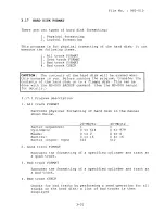
Page 87: ...s can be done with the MS DOS BACKUP command See the MS DOS manual for details 3 17 1 Program description 1 All track FORMAT Performs physical formatting of hard disk in the manner shown below 20 Mbyte 40 Mbyte Sector sequences 1 1 Cylinders 0 to 614 0 to 979 Heads 0 to 2 0 to 4 Sectors o to 16 o to 16 Sector length bps 512 512 2 Good track FORMAT Executes the formatting of a specified cylinder an...

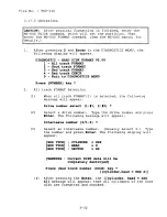
Page 88: ...rack FORMAT Selection 1 When all track FORMAT l is selected the following message will appear Drive number select 1 11 2 12 2 Select a drive number Type the drive number and press Enter The following message will appear Interleave number 3 1 3 3 Select an interleave number Usually select 3 Type the number and press Enter The following display will appear HOD TYPE HOD TYPE HOD TYPE CYLINDER HEAD SE...

Page 89: ...ually select 3 Type the number and press Enter The following message will appear HOD TYPE HOD TYPE HOD TYPE CYLINDER HEAD SECTOR XXX X XX Press track number CCCH key 4 Type a track number four digits and press Enter The first three digits are the cylinder number and the last digit is the head number This executes the formatting of good tracks or bad tracks NOTE This program can format only one tra...

Page 90: ...e will appear Interleave number 3 1 3 3 Select an interleave number Usually select 3 Type the number and press Enter When the following message appears and bad tracks of the hard disk are checked HOD TYPE HOD TYPE HOD TYPE CYLINDER HEAD SECTOR XXX X XX cylinder head XXX XX 4 After checking the bad tracks of the hard disk the Format complete message will appear 5 Press the Enter to return to the HA...

Page 91: ... heads to safe areas These areas called landing zone NOTE The built in hard disk drive controls automatically the heads to move to the landing zone at power down 3 18 2 Operations 1 After pressing 3 and Enter in the DIAGNOSTICS MENU the program is automatically executed and the following message will appear Landing seek completed HOD 1 Press Enter key 2 After pressing Enter the DIAGNOSTICS MENU ap...

Page 92: ... and Enter in the DIAGNOSTICS MENU the following message will appear DIAGNOSTIC FLOPPY DISK HEAD CLEANING VX XX Mount cleaning disk s on drive s Press any key when ready 2 After above message appears remove the Diagnostics disk insert the cleaning disk and press any key 3 When the Cleaning start message appears FDD head cleaning will begin 4 When cleaning is finished the display automatically retu...

Page 93: ...e POWER switch is turned off the error information will be lost The error information itself is displayed as the following 1 Error count CNT 2 Test name TEST 3 Subtest number NAME 4 Pass count PASS 5 Error status STS 6 Address FOO HOO 1 or memory AOOR 7 Write data WO 8 Read data RD 9 Error status name This program can store data on a floppy disk or output information to a printer 3 37 ...

Page 94: ...ount Write data Error status name Subtest number Test name Error count 1 Next 2 prev 3 Exit 4 Clear 5 Print 6 FD LogRead 7 FD LogWrite 2 Error information displayed on the screen can be manipulated with the following key operation The 1 key scrolls the display to the next page The 2 key scrolls the display to the previous page The 3 key returns the display to the DIAGNOSTIC MENU The 4 key erases a...

Page 95: ...ring FDD testing 1 Remove the diagnostics disk and insert the work disk into the floppy disk drive 2 After pressing 6 and Enter in the DIAGNOSTIC MENU the following message will appear Printer wrap around test YIN 3 Select whether to execute the printer wraparound test Yes or not No Type Y or N and press Enter If Y is selected a wraparound connector must be connected to the printer connector on th...

Page 96: ...es 9 sectors track 2 2DD Double sided double density double track 96 135 TPI MFM mode 512 bytes 9 sectors track 3 2HD Double sided high density double track 96 135 TPI MFM mode 512 bytes 18 sectors track 2 COpy This program copies from sours floppy disk to target floppy disk 3 DUMP This program displays the contents of floppy disks both 3 5 and 5 25 and hard disk designated sectors 3 22 2 Operatio...

Page 97: ...rning Disk data will be destroyed Insert work disk in to drive A Press any key when ready 4 Remove the diagnostics disk from the FDD and insert the work disk press any key The following message will appear formatting is then executed FDD TYPE FDD TYPE FDD TYPE Format start TRACK HEAD SECTOR XXX X XX track head XXX X After the floppy disk is formatted the following message will appear Format comple...

Page 98: ...memory FDD TYPE FDD TYPE FDD TYPE Copy start TRACK HEAD SECTOR XXX X XX Insert target disk into drive A Press any key when ready track head XXX XX 4 Remove the source disk from the FDD and insert the work disk formatted press any key The track head XXX X message will appear then start the copy to work disk When coping cannot be done with one operation message 2 is displayed again Repeat the operat...

Page 99: ... message will then appear Insert source disk into drive A Press any key when ready 5 Remove the diagnostics disk from the FDD and insert a source disk press any key The Track number message will then appear Type the track number and press Enter 6 The Head number message will then appear Type the head number and press Enter 7 The Sector number message will then appear Type the sector number and pre...

Page 100: ...rives 7 A number of printer ports 8 Co processor presents or not 9 Extended memory size 3 23 2 Operations After pressing 8 and Enter key to select from the DIAGNOSTICS MENU the following display will appear SYSTEM CONFIGURATION BIOS ROM VERSION X XX 640KB MEMORY PLASMA DISPLAY 1 FLOPPY DISK DRlVE S 2 ASYNC ADAPTER S 1 HARD DISK DRlVE S 1 PRINTER ADAPTER S 0 MATH CO PROCESSOR OOOOKB EXTENDED MEMORY...

Page 101: ...port IRQ level CGA SO 2S None Output port 3ESh 4 IRQ 3 IRQ 5 IRQ base address base address base address i J moves between items selects value F1 exists FS sets default FlO records changes 960 010 3FSh 2FSh 3ESh This menu above shows an example of setup options as they may be currently stored in memory Notice that selecting the type of diskette drive is not an option The T3100e automatically determ...

Page 102: ...ption s go to the next section Manual Reset 3 If the new values are correct press Fl The system restarts Manual Reset Follow these steps to change any option s manually 1 Notice the cursor reverse display highlight bar This cursor indicates which option is selected for change 2 Use the up and down arrow keys or Enter to move the cursor between options 3 When the cursor highlights the value of an o...

Page 103: ...ng lines 11 Cy1 615 H 4 S T 17 Cap 20MB 12 Cyl 980 H 5 S T 17 Cap 40MB No Drive Drive Table Abbreviation Cyl H SIT Cap Meaning cylinder head sector track capacity Select type 11 for the T3100e or type 12 for the T3100e 40 NOTE Automatic Reset sets correct Hard Disk Type automatically but once the CMOS configuration error occurs the default value is forced to type 11 In the case you have to select ...

Page 104: ...extended memory You specify 0 5MB of extended memory The system automatically allocates 1 5MB as expanded memory You have the memory kit installed there s a maximum of 4MB available for extended memory You specify 2MB of extended memory The system automatically allocates 2MB as expanded memory o Specify how you want to use the T3100e s remaining memory usually 384KB This is the system memory not a...

Page 105: ...xpanded memory Tota Extended size va ues Memory blank 384KB 384KB value above Value above Tota E anded OKB value above 384KB value above Setting system memory size to 512KB increases these values by 128KB 3 Internal KB type This option determines which keyboard scan codes the T3100e uses the standard AT scan codes or enhanced AT scan codes 84 Keys selects standard AT scan codes This is the preset ...

Page 106: ...ont specifies the Canadian French font This option lets you define the types of internal or external display adaptor card you have attached to the T3l00e You only specify this option when you install an optional video card in one of the expansion slots The setup program displays your choices a line at a time as follows Internal CGA 80 25 Internal CGA 40 25 External CGA 80 25 External CGA 40 25 Ext...

Page 107: ...orts four types of option cards None No cards are installed in the expansion Toshiba Modem Card Interface Card for Toshiba expansion chassis Others 8 Printer Port slot A Toshiba modem card is installed in the expansion slot A Toshiba expansion chassis interface card is installed in the expansion slot Another type of card is installed in the expansion slot This option specifies which type of parall...

Page 108: ...rrupt Level 3 4 5 I O Address 2F8H 3F8H 3E8H or 338H The first setup item in the serial port setup menu sets the I O address for the serial port that is to be given an interrupt level of 5 The SETUP program displays one of the following addresses as the possible I O address 3E8H 338H You can select the appropriate ones with the left and right arrow keys The second through fourth items in the seria...

Page 109: ...d When using a Toshiba modem card you have to set the setup item Option 7 Card type in Expansion slot to specify Toshiba Modem Card You also need to set the optional port IRQ level according to the I O address or interrupt level of the modem card that is specified by the communication software to be used For example set the serial port interrupt levels as shown below when the communications softwa...

Page 110: ...conflict with that of the serial A and B For example set the serial port interrupt levels as shown below when the I O address of the modem card is 2F8H or Serial A IRQ level 4 Serial B IRQ level 5 Optional port IRQ level 3 Serial A IRQ level 4 Serial B IRQ level Optional port IRQ level 3 3 54 ...

Page 111: ...und connector 2 RS 232 C Wraparound connector 3 3 TRANSMIT DATA 7 REQUEST TO SEND r 4 DATA TERMINAL READY RECEIVE DATA 2 CLEAR TO SEND 8 CARRIER DETECT 1 DATA SET READY 6 RING INDICATE 9 Figure 3 2 RS 232 C wraparound connector RS 232 C direct cable 9 pin to 9 pin 3 TD RD 2 4 DTR DSR 6 CTS 8 RI 9 7 RTS CD 1 5 GND GND 5 2 RD TD 3 1 CD RTS 7 6 DSR DTR 4 8 CTS 9 RI Figure 3 3 RS 232 C direct cable 9 ...

Page 112: ...No 960 010 4 RS 232 C direct cable 9 pin to 25 pin 1 CD RTS 2 RD TD 3 TD RD 4 DTR CTS 5 GND 7 RTS DSR RI 6 DSR 8 CTS GND CD DTR 9 RI 4 2 3 5 6 22 7 8 20 Figure 3 4 RS 232 C direct cable 9 pin to 25 pin 3 56 ...

Page 113: ... in mind 960 010 1 The system should never be disassembled unless there is a problem abnormal operation etc 2 Only approved tools may be used 3 After deciding the purpose of replacing the unit and the procedures required do not carry out any other procedures which are not absolutely necessary 4 B sure to turn the power switch off before beginning S Be sure to disconnect the AC cord and all externa...

Page 114: ... 960 010 4 2 REMOVING REPLACING THE KEYBOARD AND SPEAKER 1 Unplug the AC power cord from the system unit 2 Turn the system unit upside down and stand the handle A 3 Remove the 3 screws B 8 Figure 4 1 Base 4 2 ...

Page 115: ...Remove the keyboard C by disengaging from 6 latches D on the base E 5 Remove the shield plate F by removing 2 screws G 6 Disconnect the keyboard cable H from the system board PJ3 Figure 4 2 Keyboard and shield plate 4 3 ...

Page 116: ...File No 960 010 7 Disconnect the speaker connector I from the system board then remove the speaker J by disengaging from 2 tabs K I Figure 4 3 Speaker 8 Reverse procedure to install 4 4 ...

Page 117: ...UPPORT BOARD 1 Unplug the AC power cord from the system unit 2 Remove the mask panel A by removing 2 screws B 3 Remove the extension board cover C by removing screw D and disengaging from 2 latches E on the base F F Figure 4 4 Extension board cover 4 5 ...

Page 118: ...then remove the T3100 support board I G r J J Of I iiiM ii OW i wmo l D 1I lIIUm I n q 1 1 0 00 0 J Figure 4 5 T3100 support board 4 Reverse procedure to install NOTE To attach the IBM hafl size board 8 bit use the big size s cover included in the package To attach the Toshiba size card Use the normal cover 4 6 ...

Page 119: ...pen the plasma display 3 Using tweezers peel off the label A and keep it in a clean place 4 Remove 2 screws B fixing the PDP mask C by holding bottom D and lifting up Figure 4 6 PDP mask 5 Reverse procedure to install NOTE Confirm that the PDP mask is locked into the PDP cover with the six latches E 4 7 ...

Page 120: ...PDP mask according to section 4 4 2 Remove 4 screws A fixing the PDP unit B 3 Lift up the PDP unit then gently put it on the keyboard 4 Disconnect the three cables C from the plasma display board D B Figure 4 7 Removing the PDP unit 5 Reverse procedure to install 4 8 ...

Page 121: ... BOARD 1 Remove the PDP mask and PDP unit according to sections 4 4 and 4 5 2 Unlatch the latch A then remove the LED board B from the latch C 3 To remove the LED board disconnect the cable D Figure 4 8 LED board 4 Reverse procedure to install 4 9 ...

Page 122: ...File No 960 010 4 7 REMOVING REPLACING THE PDP COVER 1 Unplug the AC power cord from the system unit 2 Turn the system unit upside down 3 Remove the 5 screws A Figure 4 9 Base 4 10 ...

Page 123: ...4 4 through 4 6 5 Remove 3 screws B in the figure 4 13 according to section 4 8 Lift up PDP cover and top cover together and press the cable guide B nail out from the other side 6 Remove the stopper plate C by removing 2 screws D and flat head screw E C Figure 4 10 Stopper plate and cable guide 4 11 ...

Page 124: ... G from 2 hinges F and remove the ground wire H by removing a screw I 8 Remove the PDP cover J by shift 2 hinges to inside then turn the PDP cover down and lift it up Figure 4 11 PDP cover and hinges 9 Reverse procedure to install 4 12 ...

Page 125: ...play power cable K to your right and the LED board cable L and plasma display signal cable M to your left as shown in figure 4 12 2 Put the cable guide in the top cover then place each cable in the two ditches N of the PDP cover assembly as shown in figure 4 12 L N M I I I I I K N Figure 4 12 Cable position 4 13 ...

Page 126: ...d the PDP unit the LED board and the PDP cover according to sections 4 2 and 4 5 through 4 7 2 Remove the top cover A by removing 3 screws B B A Figure 4 13 Top cover 4 Reverse procedure to install NOTE Confirm that the top cover is locked into the base with 5 latches C 4 14 ...

Page 127: ...fter power off 1 Remove the keyboard PDP mask PDP unit LED board and PDP cover with top cover according to sections 4 2 and 4 4 through 4 8 2 Disconnect a connector A from the power supply board PJ4 3 Remove the power supply unit B by removing 5 screws e lift up it then disconnect the connecter D from the system board PJ7 C r A 0 Figure 4 14 Power supply unit 4 Reverse procedure to install 4 15 ...

Page 128: ... screw and washer assemblies A while lifting the power supply cover B slightly 3 Remove the power supply cover by disengaging from 3 tabs C on the power supply base D Figure 4 15 Power supply cover 4 Reverse procedure to install NOTE In case of installing place the power supply cover between the power supply base and the installing plate E and slide then attach with screws after tabs enter 4 16 ...

Page 129: ...e the disk support A by removing 2 screws B 3 Lift the disk support then disconnect 4 connectors C from the system board D 4 Remove the plasma sensor E by removing flat head screw F 5 Disconnect the battery connector G from the system board then remove the lithium battery H fixed on the system board with a snap on fastener Figure 4 16 Disk support plasma sensor and lithium battery 6 Reverse proced...

Page 130: ... LED board PDP cover with top cover power supply unit and disk support according to sections 4 2 4 4 through 4 9 and 4 11 2 Remove FDD A by removing 2 screws B and 2 special screws C from the disk support D C t A B Figure 4 17 FDD 3 Reverse procedure to install 4 18 ...

Page 131: ...DP unit LED board PDP cover unit with top cover power supply unit and disk support according to sections 4 2 4 4 through 4 9 and 4 11 2 Remove the HOD A by removing 4 special screws B from the disk support C Figure 4 18 HOD 3 Reverse procedure to install 4 19 ...

Page 132: ...ctions 4 2 4 4 through 4 7 4 9 and 4 11 2 Remove the right cooling fan A by lifting the cooling fan stopper B after unlatching the latches C 3 Disconnect the connector D from the system board PJ14 then remove the left cooling fan F by lifting the cooling fan stopper after unlatching the latches E 0 Figure 4 19 Cooling fans 4 Reverse procedure to install 4 20 ...

Page 133: ...pport and cooling fans according to sections 4 2 4 4 through 4 9 4 11 and 4 14 2 Remove the left and right cooling fan holder A by lifting them after removing 2 screws B 3 Remove the handle C by shifting toward the front and pullout after removing the cooling fan holders B A Figure 4 20 Cooling fan holder and handle 4 Reverse procedure to install 4 21 ...

Page 134: ...e keyboard PDP mask PDP unit LED board PDP cover with top cover power supply unit disk support cooling fans and holders according to sections 4 2 4 4 through 4 9 4 11 4 14 and 4 15 2 Remove the system board A by removing 11 screws B Figure 4 21 System board 3 Reverse procedure to install 4 22 ...

Page 135: ...1 SYSTEM BOARD rCS APPENDIX A BOARD LAYOUT I I I o J a o J a II o J _ J a 0 a srcl o E I I TB o _ UI r ror i L LL I _ File No 960 010 1 ID UI o I B H B A Figure A I System board rCs A I ...

Page 136: ... 80286 12 Numeric data processing socket 80287 12 Real time clock MC146818 Serial input output controller NS16450 Bus controller gate array DMA controller gate array MAP controller gate array Character generator ROM PLC controller gate array Super integration T9761 Super integration M5M82C800 Variable frequency oscillator MB4108A A 2 ...

Page 137: ... G I L 2 SYSTEM BOARD CONNECTORS I I I II r 1ft o 1 N F E M I n o J IL Sl d o J IL File No 960 010 8 A D DIS D D Figure A 2 System board connectors A 3 ...

Page 138: ...xpansion bus connector 60 pin E PJ5 8 bit slot F PJ6 HDD power connector G PJ7 Power supply connector H PJ8 FDD connector I PJ10 Serial A I F connector J PJll HDC I F connector K PJ12 PDP LED I F connector L PJ13 PRT FDD connector M PJ14 Cooling fan connector N PJ15 CRT I F connector 0 PJ17 PDP sensor switch connector A 4 ...

Page 139: ...3 0 MEMORY BOARD D tl Ie II U lUI lUI lUI 8 0 o D C I _E r J 0 I I 1 1 L J z HH _ Figure A 3 Memory board A 5 File NO 960 010 ...

Page 140: ...ector B System RAMs C KBC Keyboard controller 8742 or 8042 D System BIOS ROMs E GA EMS2 EMS controller gate array F PJl Selector connector G PJ2 Tenkey IfF connector H PJ3 Keyboard IfF connector I PJ6 Speaker connector J Sl A B PRT switch A 6 ...

Page 141: ...tor 40 pin Table B 3 Expansion bus connector pin assignment 40 pin Pin Siqnal Ilo Pin Sianal Ilo 1 IRQI0 100 I 2 IRQ14 100 I 3 SD8 100 I O 4 SD9 100 I O 5 IRQll 100 I 6 SDI0 100 I O 7 SDll 100 I O 8 SD12 100 I O 9 IRQ12 100 I 10 GND 11 SD13 100 I O 12 SD14il00 I O 13 IRQ6il00 I 14 SD15il00 I O 15 A22 100 I O 16 A23 100 I O 17 DRQ2 100 I 18 A21 100 I O 19 A19 100 I O 20 A20 100 I O 21 DACK5 000 0 2...

Page 142: ...O 20 SA9 100 I O 21 SA10 100 I O 22 SA11 100 I O 23 SA12 100 I O 24 SA13 100 I O 25 SA14 100 I O 26 SA15 100 I O 27 GND 28 SA16 100 I O 29 SA17 100 I O 30 SA18 100 I O 31 SA19 100 I O 32 SDO 100 I O 33 SD1 100 I O 34 SD2 100 I O 35 SD3 100 I O 36 GND 37 SD4 100 I O 38 SD5 100 I O 39 SD6 100 I O 40 SD7 100 I O 41 SMEMW OOO 0 42 SMEMR 000 0 43 GND 44 IOW OOO I O 45 IOR OOO I O 46 TC 100 0 47 BALE 10...

Page 143: ...SA9 100 I O 23 SA8 100 I O 24 SA7 100 I O 25 SA6 100 I O 26 SA5 100 I O 27 SA4 100 I O 28 SA3 100 I O 29 SA2 100 I O 30 SA1 100 I O 31 SAO 100 I O 1 6 PJ 5B 8 bit Slot Table B 6 8 bit slot pin assignment Pin Sianal I O Pin Sianal I O 1 GND 2 RESET 101 0 3 VCC 4 IRQ9 100 I 5 M5V 6 DRQ2 100 I 7 M12V 8 OWAIT OOO I 9 P12V 10 GNO 11 SMEMW OOO 0 12 SMEMR OOO 0 13 IOW OOO I O 14 IORiOOO I O 15 DACK3iOOO ...

Page 144: ...1 P12V I 2 GND 3 M12V I 4 M5V I 5 GND 6 GND 7 VCC I 8 VCC I 1 9 PJ 8 FDD Connector TABLE B 9 FDD Connector Pin Assignment PIN SIGNAL I O PIN SIGNAL I O 1 VCC 0 2 INDEXiOOO I 3 VCC 0 4 FDSELAiOOO 0 5 VCC 0 6 DSKCHGiOOO I 7 VCC 0 8 READY i 000 I 9 NOTCHOiOOO I 10 MONAiOOO 0 11 LOWDNSiOOO 0 12 FDCDCRiOOO 0 13 GND 14 STEPiOOO 0 15 GND 16 WDATAiOOO 0 17 GND 18 WGATEiOOO 0 19 GND 20 TRACKOiOOO I 21 GND ...

Page 145: ...nal I O 1 HRESET OOl 0 2 GND 3 HSD7 100 I O 4 HSD8 100 I O 5 HSD6 100 I O 6 HSD9 100 I O 7 HSD5 100 I O 8 HSD10 100 I O 9 HSD4 100 I O 10 HSD11 100 I O 11 HSD3 100 I O 12 HSD12 100 I O 13 HSD2 100 I O 14 HSD13 100 I O 15 HSD1 100 I O 16 HSD14 100 I O 17 HSDO 100 I O 18 HSD15 100 I O 19 GND 20 N C 21 N C 22 GND 23 HIOW OOl 0 24 GND 25 HIOR OOl 26 GND 27 N C 28 N C 29 N C 30 GND 31 IRQ14 100 I 32 HI...

Page 146: ...0 25 LEDNUM 020 0 26 LEDSCR 020 0 1 13 PJ 13 PRT FDD Connector Table B 13 PRT FDD connector pin assignment For PRTl For EXT FOOl Pin Sianal I O Sianal I O 1 STROBE OOO 0 READY 100 I 2 PDO 110 0 INDEX OOO I 3 PDl 110 0 TRACKO OOO I 4 PD2 110 0 WPROTC OOO I 5 PD3 110 0 RDDA OOO I 6 PD4 110 0 DSKCHG OOO I 7 PD5 110 0 8 PD6 110 0 9 PD7 110 0 10 ACK OOO I SWFDB OOO 0 11 BUSY 100 I SWMONB OOO 0 12 PE 10...

Page 147: ... Siqnal I O Pin Siqnal I O 1 GND 2 VCC 0 3 PDPON 100 I 2 MEMORY BOARD 2 1 IS lOlA Option Memory I F Connector Table B 17 Option memory I F connector pin assignment Pin Siqnal I O Pin Sianal I O 1 VCC 0 2 CASH OOO 0 3 MDB 100 I O 4 MAO 100 0 5 MA1 100 0 6 MD9 100 I O 7 MA2 100 0 8 MA3 100 0 9 GND 10 MAI0 100 I O 11 MA4 100 0 12 MA5 100 0 13 MD11 100 I O 14 MA6 100 0 15 MA7 100 0 16 MD12 100 I O 17 ...

Page 148: ...0 I O 24 ASL256 000 I 25 MD7 100 I O 26 PDOL 100 I 27 RASA 000 0 28 ASL1M 000 I 29 PDINL 100 0 30 VCC 0 2 3 IS 102A Option Memory I F Connector Table B 19 Option memory I F connector pin assignment Pin Sianal I O Pin Sianal I O 1 VCC 0 2 CASH OOO 0 3 MDB 100 I O 4 MAO 102 0 5 MA1 102 0 6 MD9 100 I O 7 MA2 102 0 8 MA3 102 0 9 GND 10 MD10 100 I O 11 MA4 102 0 12 MA5 102 0 13 MD11 100 I O 14 MA6 102 ...

Page 149: ...MA9 102 0 19 GND 20 MD5 100 I O 21 MEMWE 000 0 22 GND 23 MD6 100 I O 24 BSL256 000 I 25 MD7 100 I O 26 PDOL 100 I 27 RASB OOO 0 28 BSLIM OOO I 29 PDINL I00 0 30 vcc 0 2 5 PJ 1 Selector Connector Table B 21 Selector connector pin assignment Pin Sianal I O Pin Sianal I O 1 GND 2 FD2 000 I 3 VCC 0 4 FD2MB 000 I 5 VCC 0 6 F2HD 000 I 2 6 PJ 2 Tenkey I F Connector Table B 22 Tenkey I F connector pin ass...

Page 150: ...C9 000 0 13 KBSC10 000 0 14 KBRTNO OOO I 15 KBRTN1 000 I 16 KBRTN2 000 I 17 KBRTN3 000 I 18 GND 19 KBRTN4 000 I 20 KBRTN5 000 I 21 KBRTN6 000 I 22 KBRTN7 000 I 2 8 PJ 6 Speaker Connector Table B 24 Speaker connector pin assignment 3 LED BOARD 3 1 PJ 501 FH1LED Connector Table B 25 FH1LED connector pin assignment Pin Sianal IIO Pin Sianal IIO 1 GND 2 DRVALD OOO I 3 DRVBLD OOO I 4 CRTLED OOO I 5 VCC...

Page 151: ... 101 IRQ12 101 0 10 GND SD13 101 I O 12 SD14 101 IRQ6i101 0 14 SD15i101 A22i101 I O 16 A23i101 DRQ2 101 0 18 A21i101 A19i101 I O 20 A20i101 DACK6 001 I 22 GND REFRSH OOl I O 24 A18 101 MASTER 001 0 26 A17i101 SBHE OOl I O 28 IOCHKi001 MEM16 001 0 30 GND I016i001 0 32 DACK2 001 DRQ6i101 0 34 DRQ5i101 DACK5 001 I 36 MEMRi 001 IRQ4i101 0 38 MEMWi 001 IR07 101 0 40 GND I System board T3100 support boa...

Page 152: ... O 20 SA9 101 SA10 101 I O 22 SA11 101 SA12 101 I O 24 SA13 101 SA14 101 I O 26 SA15 101 GND 28 SA16 101 SA17 101 I O 30 SA18 101 SA19 101 I O 32 SDO 101 SD1 101 I O 34 SD2 101 SD3 101 I O 36 GND SD4 101 I O 38 SD5 101 SD6 101 I O 40 SD7 101 SMEMW OOl I 42 SMEMR OOl GND 44 IOW 010 IOR OOl I O 46 TC 101 BALE 101 I 48 RESET 102 DACK1 001 I 50 IRQ9 101 GND 52 VCC SYSCLK lll I 54 IRQ5 101 DRQ 101 0 56...

Page 153: ...10 GND SD13 101 I O 12 SD14 101 IRQ6 101 I 14 SD15 101 A22 101 I O 16 A23 101 DRQ2 101 I 18 A21 101 A19 101 I O 20 A20 101 DACK6 001 0 22 GND REFRSH OOl I O 24 A18 101 MASTER 001 I 26 A17 101 SBHE OOl I O 28 IOCHK OOl MEM16 001 I 30 GND 1016 001 I 32 DACK2 001 DRQ6 101 I 34 DRQ5 101 DACK5 001 0 36 MEMR OOl IRQ4 101 I 38 MEMW OOl IRQ7 101 I 40 GND I Option card T3100 support board 0 T3100 support b...

Page 154: ...9 101 SA10 101 I O 22 SAll lOl SA12 101 I O 24 SA13 101 SA14 101 I O 26 SA15 101 GND 28 SA16 101 SA17 101 I O 30 SA18 101 SA19 101 I O 32 SDO lOl SD1 101 I O 34 SD2 101 SD3 101 I O 36 GND SD4 101 I O 38 SD5 101 SD6 101 I O 40 SD7 101 SMEMW OOl 0 42 SMEMR OOl GND 44 IOW OlO IOR OOl I O 46 TC lOl BALE 101 0 48 RESET 102 DACK1 001 0 50 IRQ9 101 GND 52 VCC SYSCLK lll 0 54 IRQ5 101 DRQ lOl I 56 DACK3 0...

Page 155: ...b r File No 960 010 C 0 E F LJ I ex 3 rr 3 esc 5 a 0 I U f tL IT _ 4 fT 40 T d tao nr r b L r 5 5 E U e u a 0 N F J J 6 6 F V f v a Q a I 7 t 7 GW 9 w t 8 H X h x 90 l 9 I Y y A JZj z B 0 K k c L L I o M m E A N 1 n rv F 0 o C l u 0 11 e Y G R e 6 I bl rFf I i lJ APt0d o A f T 2 0 e n c5 r con p 2 E I nl ...

Page 156: ...File No 960 010 C 2 ...

Page 157: ...9 16 I Q I 10 71 17 I Will 77 18 I E I 12 65 19 I R I 13 72 20 I T I 14 74 21 I Y I 15 79 22 I U I 16 75 23 I I I 17 69 24 I 0 I 18 6F 25 I P I 19 70 26 I I lA 5B I I 27 I I lB 5D I I 28 IEnterl lC OD 29 ICtrl I 30 I A I lE 61 31 I S I iF 73 32 I 0 I 20 64 33 I F I 21 66 34 I G I 22 67 D l Capl Key No 1 Top 35 I H Lower Case 23 68 36 I J I 24 6A 37 I K I 25 6B 38 I L I 26 6C 39 I I 27 3B I I 40 I ...

Page 158: ...3B 00 60 I F2 I 3C 00 61 I F3 I 3D 00 62 I F4 I 3E 00 63 I F5 I 3F 00 64 I F6 I 40 00 65 I F7 I 41 00 66 I F8 I 42 00 67 I F9 I 43 00 68 I FlO I 44 00 69 INurn I ILock I 70 IScrol I I Lockl 71 IHorne I 47 00 72 I 1 48 00 73 IPgUp I 49 00 Capl Key No I Top 75 I 77 I Lower Case 4B 00 4D 00 79 I End I 4F 00 80 I v 50 00 81 IPgDn I 51 00 82 I Ins I 52 00 83 I Del I 53 00 84 I Sys I I Req I 85 I Fn D 2...

Page 159: ...APPENDIX E KEY LAYOUT Figure E l USA version E l File No 960 010 ...

Page 160: ...File No 960 010 2 UK VERSION Figure E 2 UK version E 2 ...

Page 161: ...File No 960 010 3 GERMANY VERSION Figure E 3 Germany version E 3 ...

Page 162: ...File No 960 010 4 FRANCE VERSION Figure E 4 France version E 4 ...

Page 163: ...File No 960 010 S SPAIN VERSION Figure E S Spain version E S ...

Page 164: ...File No 960 010 6 ITALY VERSION Figure E 6 Italy version E 6 ...

Page 165: ...7 SCANDINAVIAN VERSION 9 mm1 m8 R i 3 J I _ jj Jt f ft gO QJ i go Q 8 j 8 DfGJ File No 960 010 flI M M a uS g g FJJ iJ f1 Jlt f1 l Figure E 7 Scandinavian version E 7 ...

Page 166: ...File No 960 010 S SWITZERLAND VERSION Figure E S Switzerland version E S ...

Page 167: ...File No 960 010 9 KEYCAP NUMBERS Figure E 9 Keycap number E 9 ...

Reviews: