background image


TB9051FTG 

Ver.1.1 2019-03-14 

18 / 49

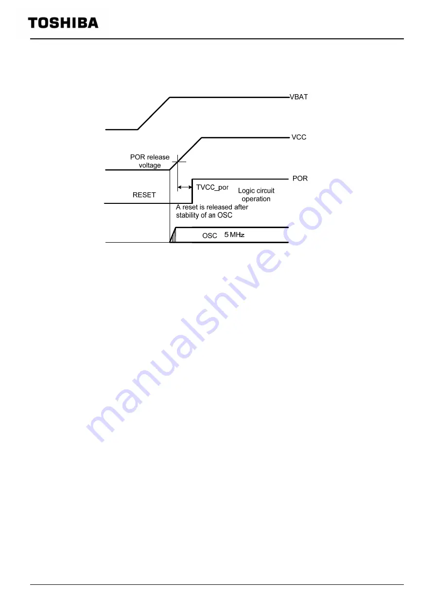
7.5. OSC circuit (oscillation circuit) 

An OSC circuit consists of CR oscillators of internal resistance and an internal capacitor, and performs a 

5 MHz (typ.) oscillation. 

Without a trigger of oscillation starting, a oscillation starts automatically according to the rise of supply 

voltage(VCC). 


Fibure 7.5-1    Operation at the time of OSC circuit starting 


Note: Some of timing charts in this document may be omitted or simplified for explanatory purposes. 


Summary of Contents for TB9051FTG

Page 1: ...rrors 3 Feature Motor driver block Single channel H Bridge driver Ron Pch Nch 0 45 Ω Max Tj 150 C VBAT 8 V Abnormality detection function Over current detection over temperature detection VBAT undervoltage detection VCC undervoltage detection and VCC high voltage detection Built in initial diagnosis function Power supply abnormality detection circuit VBAT undervoltage VCC undervoltage and VCC high...

Page 2: ...rcuit However each EN and ENB signal is connected independently to the output circuit of each driver Control Over current detection POR Low voltage detection High voltage detection Thermal detection Pre Driver Over temperature detection Over current detection Hi side current monitoring VBAT OUT1 OUT2 PGND AGND PWM2 PWM1 EN ENB M Battery Microcontroller 5V ECU VCC DIAG OSCcircuit OCC OCM EN circuit...

Page 3: ...TB9051FTG Ver 1 1 2019 03 14 3 49 5 Pin Assignment Pin assignment Top View Figure 5 1 Pin assignment ...

Page 4: ... which flows from the voltage generated to an external resistor into the H side 8 PWM1 Driver control signal input pin 1 9 PWM2 Driver control signal input pin 2 11 12 24 25 VBAT Battery power supply 13 14 OUT1 H bridge driver output pin 1 15 16 17 19 20 21 PGND Power ground pin used as the ground of H bridge 18 DIAG Diagnostic signal output pin Open drain type of output pin 22 23 OUT2 H bridge dr...

Page 5: ...side GND side OCC Pull down I 6 B AGND ENB Pull up I 6 B AGND EN Pull down I 6 B AGND PWM1 Pull down I 6 B AGND PWM2 Pull down I 6 B AGND OUT1 O 40 OUT2 O 40 DIAG O 6 OCM O 6 C B VCC AGND TEST1 Pull down I 6 B AGND TEST2 Pull down I 6 B AGND VBAT Power supply 40 A AGND PGND VCC Power supply 6 B AGND PGND NC PGND GND D AGND AGND GND D PGND Figure 6 1 Protection element type 40V PDMOS Vdss NMOS保護 PM...

Page 6: ...orm after setting the brake between them Otherwise the IC may be broken Note 2 In the current limitation control the operation is different from the above table of the motor function For details refer to current limitation control Section 7 3 Table 7 1 2 Function operation at abnormality detection PWM1 PWM2 EN ENB DIAG pin OUT1 OUT2 Over temperature detection Note Output is OFF regardless of input...

Page 7: ... may be omitted or simplified for explanatory purposes PWM function Forward timing chart in the case of short brake operation PWM1 PWM2 L D T Dead Time In order to prevent the through current by simultaneous ON of Hi side Pch Tr and Lo side Nch Tr Pch Tr off and Nch Tr off time 4 μs typ are prepared Figure 7 1 2 1 Timing chart at the time of PWM function Forward Note Some of timing charts in this ...

Page 8: ... Dead Time In order to prevent the through current by simultaneous ON of Hi side Pch Tr and Lo side Nch Tr Pch Tr off and Nch Tr off time 4 μs typ are prepared Figure 7 1 2 2 Timing chart at the time of PWM function Forward Note Some of timing charts in this document may be omitted or simplified for explanatory purposes ...

Page 9: ... Reverse timing chart in the case of short brake operation PWM1 PWM2 L D T Dead Time In order to prevent the through current by simultaneous ON of Hi side Pch Tr and Lo side Nch Tr Pch Tr off and Nch Tr off time 4 μs typ are prepared Figure 7 1 4 1 Timing chart at the time of PWM function Reverse Note Some of timing charts in this document may be omitted or simplified for explanatory purposes H L ...

Page 10: ... Dead Time In order to prevent the through current by simultaneous ON of Hi side Pch Tr and Lo side Nch Tr Pch Tr off and Nch Tr off time 4 μs typ are prepared Figure 7 1 4 2 Timing chart at the time of PWM function Reverse Note Some of timing charts in this document may be omitted or simplified for explanatory purposes ...

Page 11: ...operation At the time of VCC undervoltage POR detection X X L High Z High Z 1 For the clearing condition of the DIAG output latch refer to Section 7 7 1 DIAG function release operation after the over temperature detection at the time of the over temperature detection At the time of the over current detection refer to the Section 7 8 3 Timing chart of restart from the motor output OFF state at the ...

Page 12: ...the rising edge of EN pin or the falling edge of ENB pin Moreover for the VBAT and VCC voltage abnormality they are returned automatically after returning normal voltage In the automatic returning operation the DIAG output returns the normal operation in the response to the release voltage of each power supply monitoring function If the VCC voltage is dropping still in the abnormal state L holding...

Page 13: ...g after the detection The Current Limit signal rises at the falling edge of tBLANK1 because the current flows more than Ilim H 6 5 A after passing the time tBLANK1 11 5 μs 3 After Blanking the motor drive output is set to the short brake mode lower simultaneous ON automatically Then the current is regained At the same time Toff_min also rises to H and starts counting The PWM1 signal of Note1 is ig...

Page 14: ...ion and the motor drive current is reduced by PWM1 L signal 7 3 2 Thermal Adjustment Function of Current Limitation Control When the junction temperature Tj rises in the operation of the current limitation control circuit the current limitation threshold falls to 2 5A typ after detecting Twar temperature 150 C to 170 C The Ilim L may be also lowered by falling of the threshold of Ilim H Figure 7 3...

Page 15: ... monitoring block at the time of current limitation control Note Some of the functional blocks of circuits in the block diagram may be omitted or simplified for explanatory purposes 7 3 4 Operating flow Figure 7 3 4 Operation flow of current limitation control circuit Note Some of the functional blocks or circuits in the block diagram may be omitted or simplified for explanatory purposes ...

Page 16: ...y purposes This resistance 220Ω 1 assumes in the case that the power supply of MCU ADC is 5V When the power supply of MCU is less than 5V use adjusting of ressistance value Be careful for the external resistance 220Ω Sufficient evaluation is required since not only the resistance value fluctuates but also the output voltage also fluctuates The external capacitor 2 should select whether it connects...

Page 17: ...0 3 50 4 00 4 50 5 00 5 50 6 00 6 50 OCM電流 mA 出 電流 A TB9051FTG OCM 電流特性 0 6A 仕様MIN 仕様TYP 仕様MAX 0 00 0 20 0 40 0 60 0 80 1 00 1 20 1 40 1 60 1 80 2 00 2 20 2 40 2 60 2 80 3 00 3 20 3 40 3 60 3 80 4 00 4 20 4 40 0 00 0 10 0 20 0 30 0 40 0 50 0 60 0 70 0 80 0 90 1 00 1 10 1 20 1 30 1 40 1 50 OCM電流 mA 出 電流 A TB9051FTG OCM 電流特性 0 1 5A 仕様MIN 仕様TYP 仕様MAX TB9051FTG OCM current characteristics 0 to 6A TB90...

Page 18: ...nd an internal capacitor and performs a 5 MHz typ oscillation Without a trigger of oscillation starting a oscillation starts automatically according to the rise of supply voltage VCC Fibure 7 5 1 Operation at the time of OSC circuit starting Note Some of timing charts in this document may be omitted or simplified for explanatory purposes ...

Page 19: ...s typ is built in If the VCC voltage is more than the POR detecting voltage value of VCC undervoltage even when output is in the OFF High Z state by undervoltage detection of VBAT a Logic circuit is able to operate Figure 7 6 1 1 Threshold characteristics of VBAT undervoltage detection Note Some of timing charts in this document may be omitted or simplified for explanatory purposes Figure 7 6 1 2 ...

Page 20: ...typ is built in Figure 7 6 2 1 VCC undervoltage detection and POR threshold characteristics Note Some of timing charts in this document may be omitted or simplified for explanatory purposes Figure 7 6 2 2 Timing chart of VCC undervoltage detection Note Some of timing charts in this document may be omitted or simplified for explanatory purposes Figure 7 6 2 3 POR timing chart of VCC undervoltage No...

Page 21: ...age detection a logic circuit can operate Figure 7 6 3 1 VCC high voltage detection circuit Note Some of timing charts in this document may be omitted or simplified for explanatory purposes Figure 7 6 3 2 Timing chart of VCC high voltage detection Note Some of timing charts in this document may be omitted or simplified for explanatory purposes Note The VCC high voltage detection function is not a ...

Page 22: ... automatically when being normal voltage The DIAG output returns a normal operation when the automatic return receives abnormal release signals from each power supply monitoring function Figure 7 6 4 DIAG function when VBAT and VCC voltage is abnormal Note Some of timing charts in this document may be omitted or simplified for explanatory purposes ...

Page 23: ... signals of over temperature detection circuit are made into undetected state forcibly during an initial diagnosis and a re start Note PWM input is not available at the time of TSD generation Note Some of timing charts in this document may be omitted or simplified for explanatory purposes Note The guarantee storage temperature range of the absolute maximum ratings of this product is maximum 150 C ...

Page 24: ... over temperature detection L output latch of DIAG pin is cleared at the rising edge of EN pin or the falling edge of ENBpin Figure 7 7 1 DIAG function in the over temperature detection Note Some of timing charts in this document may be omitted or simplified for explanatory purposes ...

Page 25: ...to GND tBLANK2 1μs is set to the threshold of over current Iovc and the prevention time of the malfunction is set by noise Then if a current flows longer than the setting time the output is in the OFF state After passing 500 ms typ it returns automatically and repeats operations until instructions from external MCU The OUT1 OUT2 outputs return the normal operation when an output current is in the ...

Page 26: ... current Iovc and the prevention time of the malfunction is set by noise Then if a current flows longer than the setting time the output is in the OFF state For returning from OFF state each function restarts according to input instructions from MCU Each function re starts with one pulse signal of EN falling or one pulse signal of ENB rising When tBLANK2 operates tBLANK1 is canceled In the case of...

Page 27: ...me of short to power supply short to GND and load short Note Some of timing charts in this document may be omitted or simplified for explanatory purposes Note This detection circuit is a function to avoid abnormal conditions such as output short circuit temporarily and does not guarantee that the IC does not break Therefore utmost care is necessary in the design of output lines VBAT VCC and substr...

Page 28: ...of operation those are low side regeneration operation OUT1 Nch ON OUT2 Nch ON and high side regeneration operation OUT1 Pch ON OUT2 Pch ON High side regeneration operation OUT1 Pch ON OUT2 Pch ON is done regeneration operation at the time of OUT1 OUT2 short to the power supply At the time of other detection operations it becomes low side regeneration operation OUT1 Nch ON OUT2 Nch ON Note When th...

Page 29: ... when H is input to a EN pin and L is input to a ENB pin a check result is output in the DIAG pin When a comparator circuit is a normal performance H output of DIAG is done and when there is unusual operation L output of DIAG is done L output of the DIAG is latched in the initial diagnosis control circuit The latch result is latched until VCC undervoltage POR detection or diagnosis restart operati...

Page 30: ...diagnosis operation Note Some of timing charts in this document may be omitted or simplified for explanatory purposes Figure 7 10 3 Diagnostic restart operation Note Some of timing charts in this document may be omitted or simplified for explanatory purposes ...

Page 31: ... voltage VBAT Low voltage VCC Low voltage VCC High voltage VBAT Low voltage VCC Low voltage VCC High voltage VBAT Low voltage VCC Low voltage VCC High voltage High z Initial diagnosis does not start It becomes an unusual function of Table 7 1 2 5 When at least one condition continues the state where it does not detect Abnormal L High z L Output Function 4 In the case of NG it is also at any 1 cond...

Page 32: ...oltage VCC Low voltage VCC High voltage VBAT Low voltage VCC Low voltage VCC High voltage Under diagnostic operation Abnormal L Normal L Memo Abnormal L High z L After termination of a restart High z H Output Function Diagnostic result Abnormal L High z L Output Function Output Function High z L Output Function The state where it does not detect Test 2 A threshold is changed The state where it doe...

Page 33: ...s Power dissipation PD JEDEC board 4 layers Note 7 4 7 W For the current items the current flowed into the IC is described plus and the current flowed out from the IC is described minus Note 1 Do not exceed the maximum ratings including in Back EMF Absolute maximum ratings The maximum rating is the rating that should never be exceeded even for a shortest of moments If the maximum rating is exceede...

Page 34: ... voltage difference between PGND and VBAT should be less than maximum 40V Note 6 The voltage difference between AGND and VCC should be less than maximum 6V Note 7 PCB size 114 3 mm x 76 2 mm x 1 6 mm Multi layer Cu 4 layers Cu layer area 74 74mm2 ...

Page 35: ...area of Cu 600mm2 PCB B θja 26 4 C W θjc 1 C W Junction E Pad PCB size 114 3 mm x 76 2 mm x 1 6 mm JDEC Jesd51 7 Number of layers Multi Layer Cu 4 layers Layer thickness of Cu 35μm 1 4 layers 70 μm 2 3 layers Layer area of Cu 74 x 74 mm2 Condition Power consumption 1W Ambient environment temperature 25 C Windless 0 1 1 10 100 0 001 0 01 0 1 1 10 100 1000 10000 A基板 B基板 Heat resistance C W Time sec ...

Page 36: ...upply of internal analog system and each kind of monitoring circuit The VCC undervoltage detection and VCC high voltage detection functions are also built in as the monitoring function Table 9 1 Operating range Parameter Symbol Rating Unit Note Power supply voltage VBAT 4 5 to 28 0 V The motor function can operate until VBAT undervoltage detection or VCC undervoltage detection VCC 4 5 to 5 5 Opera...

Page 37: ...H2 ENB 5 0 5 μA IIL1 ENB VIN GND 88 42 20 μA IIL2 OCC PWM1 PWM2 EN 5 0 5 μA PWM input maximum frequency Note 1 PWMMAX PWM1 PWM2 20 kHz EN ENB logic definite time TEN_ENB EN ENB Logic definite time at thte time of changing EN and ENB pin logic 5 0 μs Consumption current ICC VCC VCC 5 V Figure 11 1 2 9 5 0 mA IBAT VBAT VBAT 14 V Figure 11 1 1 0 2 0 mA Note 1 For the width of the PWM1 PWM2 use so tha...

Page 38: ...Figure 7 6 2 1 3 3 3 5 3 7 V Hysteresis width of VCC undervoltage detection VCCHLHYS VCC Figure 7 6 2 1 0 1 0 20 0 3 V VCC undervoltage detection filter TVCC_uv VCC Figure 7 6 2 2 1 56 2 5 4 2 ms VCC undervoltage detection filter at release TVCC_uv2 VCC Figure 7 6 2 2 0 100 167 μs VCC undervoltage POR detection voltage VCCRHL VCC Figure 7 6 2 1 2 85 3 07 3 25 V Hysteresis width of VCC undervoltage...

Page 39: ... OUT1 OUT2 Tj 25 C Iout 3 A VBAT 8 V 340 mΩ Tj 150 C Iout 3 A VBAT 8 V 450 Tj 150 C Iout 3 A VBAT 4 5 V 510 Output leakage current Ioutleak OUT1 OUT2 OUT1 2 OFF High Z Vout VBAT 28 V 0 100 μA OUT1 2 OFF High Z Vout GND 100 0 Output Slew Rate trD tfD OUT1 OUT2 VBAT 14 V Figure 10 9 1 0 3 0 8 1 6 μs Delay time of driver output tD on PWM1 PWM2 OUT1 OUT2 RL 3 Ω VBAT 14 V Figure 10 9 2 8 0 13 μs tD off...

Page 40: ... condition unless otherwise specified VBAT 4 5 to 28 V VCC 4 5 to 5 5 V Ta 40 to 125 C Parameter Symbol Pin name Test condition MIN TYP MAX Unit H side of current limitation threshold Ilim H OUT1 OUT2 1 8 2 5 3 5 A Current limitation temperature Note 1 Twar 150 160 170 C Detection filter of current limitation temperature Twarfil 2 66 4 0 6 67 μs Note 1 This cahacteristic is disign value It is impo...

Page 41: ...ge current of DIAG output Idiag leak DIAG Vdiag 5V 0 5 0 μA L level output voltage Vdiag DIAG RL 5 1 kΩ 0 02 0 4 V Response time Tpddiag DIAG 8 0 μs 10 8 High side current monitoring Table 10 9 Electrical characteristics of output High side current monitoring Test condition unless otherwise specified VBAT 4 5 to 28 V VCC 4 5 to 5 5 V Ta 40 to 125 C Parameter Symbol Pin name Test condition MIN TYP ...

Page 42: ...ay be omitted or simplified for explanatory purposes Figure 10 9 2 Driver output delay Note Some of timing charts in this document may be omitted or simplified for explanatory purposes Figure 10 9 3 Driver output Enable delay Note Some of timing charts in this document may be omitted or simplified for explanatory purposes PWM1 2 OUT1 2 1 5V 1 5V 80 20 tD on tD off ...

Page 43: ...lfunction from malfunction or failure Figure 11 2 tDEN test circuit Note Components in the test circuits are only used to obtain and confirm the device characteristics These components and circuits do not warrant preventing the application from malfunction from malfunction or failure VBAT OUT1 OUT2 PGND AGND PWM2 PWM1 EN ENB VCC DIAG OCC OCM 10μF 0 1μF 5 1kΩ 220Ω 1μF 0 1μF 100μF 100Ω 100Ω VBAT OUT...

Page 44: ...and this circuit can be controlled by ENB Table 12 2 Example of application circuit 2 Control OCL detection POR Low voltage detection High voltage detection Thermal detection Pre Driver Thermal detection OCL detection High side current monitoring VBAT OUT1 OUT2 PGND AGND PWM2 PWM1 EN ENB M Battery MCU 5V ECU VCC DIAG OSCcircuit OCC OCM EN circuit 5 1kΩ Low voltage detection Initial diagnosis Low v...

Page 45: ...paid to the layout of the output line VBAT VCC and GND line since IC may be destroyed due to short circuit between outputs to the power supply or to the ground Note 5 For the board design it is necessary to consider the solid pattern of AGND and PGND Back EMF While a motor is rotating there is a timing at which power is fed back to the power supply At that timing the motor current is fed back to t...

Page 46: ...TB9051FTG Ver 1 1 2019 03 14 46 49 13 Package 13 1 Package dimensions Table 13 1 Package dimensions Weight 0 22g Typ ...

Page 47: ...rt number TB9051FTG 3 Lot code e g 613QA11 4 Country Region of origin JAPAN Lot code description Example 6 13 Q A11 1 2 3 4 1 Last number of calendar year Example shows 6 of 2016 2 Week code Example shows 13th week 3 Product sight code Q 4 Toshiba management code 3 digits at maximum 613QA11 ...

Page 48: ...erate properly or IC breakdown before operation In addition depending on the method of use and usage conditions if over current continues to flow for a long time after operation the IC may generate heat resulting in breakdown 2 Thermal Shutdown Circuit Thermal shutdown circuits do not necessarily protect ICs under all circumstances If the thermal shutdown circuits operate against the over temperat...

Page 49: ...ent used in nuclear facilities equipment used in the aerospace industry and lifesaving and or life supporting medical equipment IF YOU USE PRODUCT FOR UNINTENDED USE TOSHIBA ASSUMES NO LIABILITY FOR PRODUCT For details please contact your TOSHIBA sales representative or contact us via our website Do not disassemble analyze reverse engineer alter modify translate or copy Product whether in whole or...

Reviews: