TC32306FTG
2015-10-01
50
6.
From either slower timing which after reading the third register setup, or after the output level of
Reference Clock Oscillator is over a certain level, the setup sequence and operation of internal
function blocks will start after setting Delay time.
7.
Signal Detections (RSSI & Noise Detection) with operating cycle (Initial value: 1.35 ms) set by
register will start after the internal setup (about 0.22 ms) is finished.
8.
Start timing of the demodulation output (from DATA_IO pin) is varied with Bit Rate Filter
setting, data rate or other register settings. Preamble Detection output starts after the
demodulation output is obtained.
Notice:
-
Set the configuration during the stable voltage supply.
-
Check the relationship between supply voltage and reset, when to utilize the power on reset
during boot sequence. (See the notice in 6.3.1)
6.9.2 Transition in Run Status (RX
à
TX
à
RX)
Transition of RX/TX each other in Run Status by setting the register: h’0A[D5]RX_TX.
Example: RX
à
TX
à
RX (SPI Mode)
The example of the transition “RX
à
TX
à
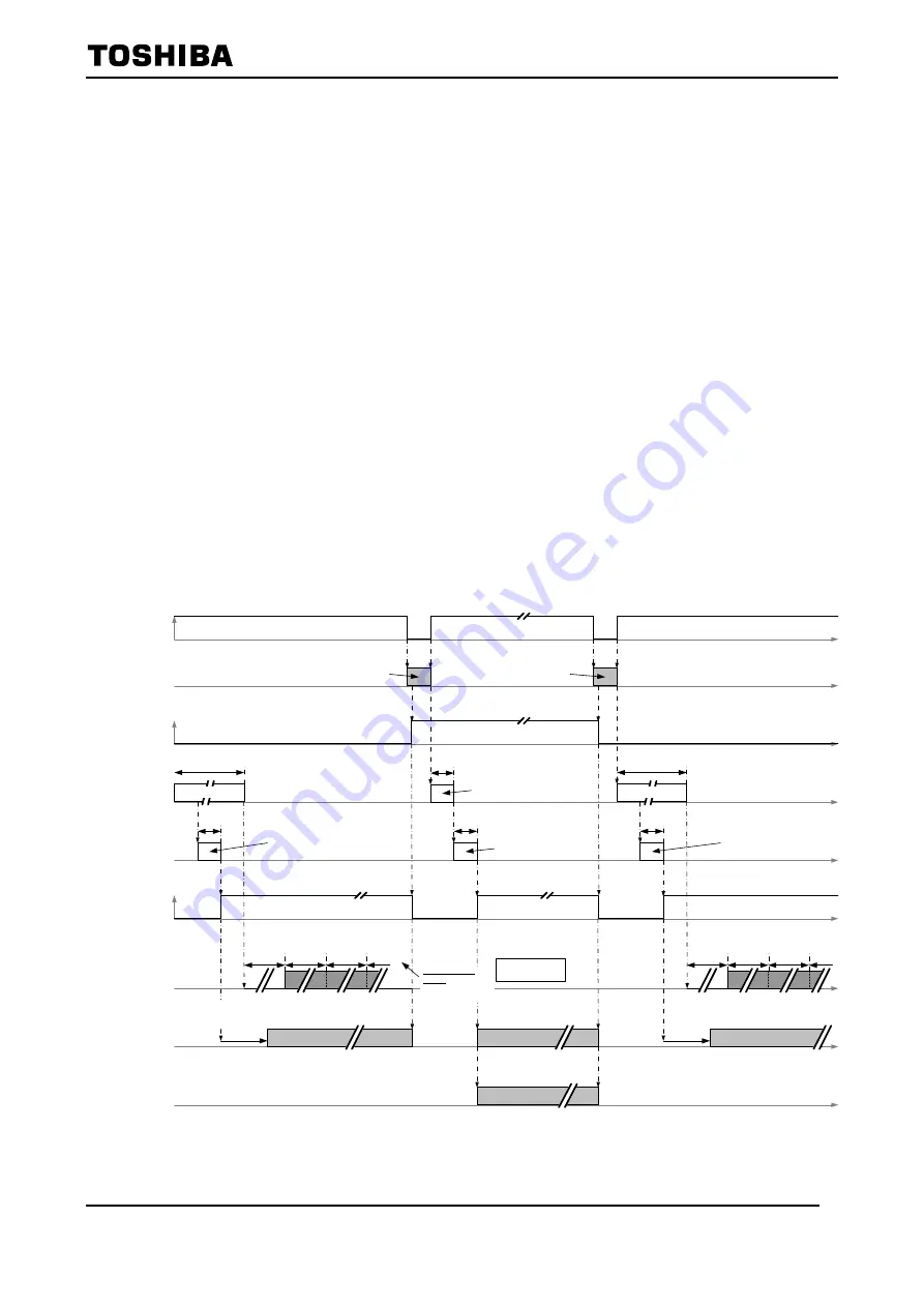
RX” in SPI Mode is shown as Fig 6-32.
1.
At the end of RX, set the register: h’0A[D5]RX_TX = ”1” then TC32306FTG changes to TX.
2.
After finishing all register settings for TX and CS pin is set to ”H”, this IC starts the setup
sequence and PLL lock-up, then this IC is operated with setting registers.
3.
At the end of TX, set the register: h’0A[D5]RX_TX = ”0” then this IC changes to RX. After
finishing all register settings for RX and CS pin is set to ”H”, this IC starts the setup sequence
and PLL lock-up, then this IC is operated with setting registers.
Fig 6-32 Example of Timing Chart (RX
à
TX
à
RX in SPI Mode)
Control Command
(
SPI
)
Internal Counter
PLL_LD Signal
: at DET_TMONI1 / 2 pin
PLL Block
h'0A[D5]RX_TX
(Initial Value = "0"àRX)
Signal Detections
(RSSI / Noise Detection)
: at DET_TMONI1 / 2 pin
CS Signal
TX Register Setting
Input
RX Register Setting
Input
About 0.22ms
Detection Setup
0.05ms
Internal Setup
About 0.22ms
Detection Setup
0.05ms
Lock Up
0.05ms
Lock Up
0.05ms
Lock Up
*: Initial Value
It indicates typical.
1.35ms
1.35ms
1.35ms
1.35ms
1.35ms
1.35ms
1.35ms
1.35ms
Demodulation Output
: at DATA_IO pin
RF Output Signal
: at PA_OUT pin
Start of the demodulation
output depends on Bit Rate
Filter setting or others.
Demodulation
Output
Modulation
Input
Demodulation
Output
Detection Cycle
Setting
* 0.338ms / 0.675ms
/ 1.35ms / 2.70ms


