background image

710CDT/720CDT

A-1

Appendix A  Handling the LCD Module

Precautions for handling the LCD module

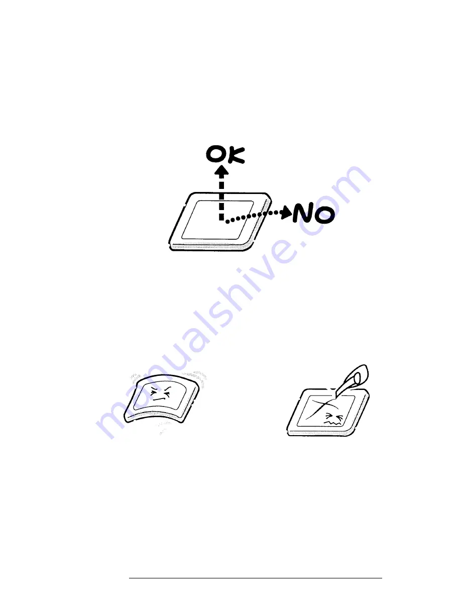
The computer's LCD module can be easily damaged during assembly or disassembly.  Observe
the following precautions when handling the module:

1.

When installing the LCD module in the LCD cover, be sure to seat it so that it is
properly aligned and maximum visibility of the display is maintained.

2.

Be careful to align the holes at the four corners of the LCD module with the corre-
sponding holes in the LCD cover before securing the module with screws.  Do not
force the module into place, because stress can affect its performance.

Also, the panel's polarized surface is easily scarred, so be careful when handling it.

3.

If the panel's surface gets dirty, wipe it with cotton or a soft cloth.  If it is still dirty,
try breathing on the surface to create a light condensate and wipe it again.

Summary of Contents for Tecra 710CDT

Page 1: ... Disk storage This computer has a 1 2 billion byte 1 13 GB removable HDD pack Selectable Bay The Selectable Bay allows connection to either a Floppy Disk Drive FDD or a CD ROM drive The FDD supports 3 5 inch 2HD 1 44 MB disks and 2DD 720 KB disks The FDD drive can be connected to an external FDD port with an attachment when the CD ROM drive is installed in the Selectable Bay A full size six speed ...

Page 2: ...ible printer or other parallel device The port supports Extended Capabilities Port ECP conforming to IEEE 1284 Serial port The serial controller is 16550UART compatible This standard 9 pin serial port can be used to connect serial devices such as a serial printer serial mouse or external modem Externalmonitorport The female 15 pin D shell connector can be connected to an external SVGA monitor This...

Page 3: ...system interface controller External FDD port The external FDD port lets you connect an external FDD device when a CD ROM drive is installed AccuPoint A pointer control stick located in the center of the keyboard provides convenient control of the cursor without requiring desk space for a mouse Serial infrared port This computer incorporates an IrDA1 0 infrared data association standard infrared t...

Page 4: ...CDT 720CDT The 710CDT 720CDT Personal Computer is shown in Figure 1 1 and their system configura tion in Figure 1 2 Figure 1 1 710CDT 720CDT personal computer Figure 1 2 710CDT 720CDT system unit configuration ...

Page 5: ... diagram The system board is composed of the following major components Intel Pentium processor operating at 133 MHz and 2 9 3 3 volts A math co processor and 16 KB cache memory are integrated into the processor Level 2 cache memory Data RAM 256 KB Two 32K x 32 bit pipe line burst synchronous SRAM chips 3 3 volt operation 8 ns access time ...

Page 6: ...B are used for password security 16 KB are used for boot strap 32 KB are reserved 5 volt operation 120 ns access time 8 bit width data transfer Optional memory One expansion memory slot for 8 16 32 64 and 128MB memory modules which consist of 1M x 16 bit chips 8 16 32MB and 4M x 16 bit chips 64 128MB EDO DRAM is used 3 3 volt operation No parity bit 60 ns access time 64 bit width data transfer Vid...

Page 7: ...array is a multiplexer for a ZV port LCD interface Gate Array This gate array controls data transfer between a VGA controller and LVDS PC Card Controller Gate Array This gate array has the following functions PC card control CardBus control ZV port support multiplex gate array control Miscellaneous Gate Array This gate array has the following functions Communicationcontrol Communication with KBC I...

Page 8: ...ard interface controller The KBC controls the internal keyboard external keyboard AccuPoint or PS 2 mouse AccuPoint Controller IPSC One KPAAC0062A chip is used The controller provides simultaneous control of both the AccuPoint and a PS 2 mouse Real Time Clock RTC One T9934 chip is used The T9934 has 128 bytes of memory Fourteen 14 bytes are used for the calendar and clock and the remaining 114 byt...

Page 9: ...D port The FDD is shown in Figure 1 4 and its specifications are listed in Table 1 1 Figure 1 4 3 5 inch FDD Table 1 1 3 5 inch FDD specifications Item 2 MB mode 1 MB mode Storage capacity KB Unformatted 2 000 1 000 Formatted 1 440 720 Number of heads 2 2 Number of cylinders 80 80 Access time ms Track to track 3 3 Average 181 181 Head settling time 15 15 Recording track density tpi 135 135 Data tr...

Page 10: ...ni winchester type magnetic heads 710CDT 720CDT supports a 1 13 GB HDD The HDD is shown in Figure 1 5 and its specifications are listed in Table 1 2 Figure 1 5 2 5 inch HDD Table 1 2 2 5 inch HDD specifications Items MK2720FC Storage capacity GB 1 216 954 368 Cylinders 2 358 Heads 16 Sectors 63 Bytes per sector 512 Rotation speed rpm 4 200 Recording method 8 9 RLL ...

Page 11: ...board controller on the system board through a 25 pin flat cable The 710CDT 720CDT AccuPoint pointer control stick located in the center of the keyboard provides convenient control of the cursor without requiring desk space for a mouse The keyboard is shown in Figure 1 6 See Appendix E for optional keyboard configurations Figure 1 6 Keyboard ...

Page 12: ... 7 and its specifications listed in Table 1 3 Figure 1 7 CD ROM drive Table 1 3 CD ROM drive specifications Item 1 x mode 6 x mode Data Capacity bytes block Mode 1 2 048 Mode 2 2 336 Transfer Rate Sustained Block transfer speed blocks s 75 450 Sustained Data transfer speed kbytes s Mode 1 150 900 Mode 2 171 1 026 ATAPI Burst Mbytes s 8 33 PIO mode 2 Access time ms Average Random Access 350 190 Ave...

Page 13: ...corporates functions of the Video Graphics Array VGA and Super VGA SVGA for external displays The display controller is F65550 and enables an LCD to display a maximum 16 million colors The TFT LCD is shown in Figure 1 8 and its specifications are listed in Table 1 4 Figure 1 8 710CDT color LCD Table 1 4 710CDT color LCD specifications Item Specifications Number of Pixels pixels 800 x 600 Dot pitch...

Page 14: ...s a high frequency current to light the LCD s Fluorescent Lamp Specifications for the FL inverter are listed in Table 1 5 Table 1 5 FL inverter board specifications for 710CDT color LCD Status Item Specifications Input Voltage V 4 to 5 5 Power W 4 8 Output Voltage Vrms 1 100 Current mA 6 0 4 0 3 6 2 4 NOTE FL currents at power on are Bright Semi bright AC adapter connected 6mA 3 6mA AC adapter not...

Page 15: ...corporates the functions of a Video Graphics Array VGA and Super VGA SVGA for external displays The display controller is F65550 and enables an LCD to display a maximum 64K colors The TFT LCD is shown in Figure 1 9 and its specifications are listed in Table 1 6 Figure 1 9 720CDT color LCD Table 1 6 720CDT color LCD specifications Item Specifications Number of Pixels pixels 1024 x 768 Dot pitch mm ...

Page 16: ...s a high frequency current to light the LCD s Fluorescent Lamp Specifications for the FL inverter are listed in Table 1 7 Table 1 7 FL inverter board specifications for 720CDT color LCD Status Item Specifications Input Voltage V 4 to 5 5 Power W 4 8 Output Voltage Vrms 1 100 Current mA 6 0 4 0 3 6 2 4 NOTE FL currents at power on are Bright Semi bright AC adapter connected 6mA 3 6mA AC adapter not...

Page 17: ...d off and detects a fully charged battery 5 Determines if the power can be turned on and off 6 Provides more accurate detection of a low battery 7 Calculates remaining battery capacity 8 Detects Ring Indicator RI signal for the Auto Power On function The power supply output ratings are specified in Table 1 8 Table 1 8 Power supply board output ratings DC Regulation Maximum Use Name voltage toleran...

Page 18: ... Main battery Lithium Ion 10 8 V 5 600 mAh Backup battery Nickel Metal Hydride 7 2 V 35 mAh RTC battery Nickel Metal Hydride 3 6 V 35 mAh 1 10 1 Main Battery BatteryChargingControl Battery charging is controlled by a microprocessor that is mounted on the power supply The microprocessor controls whether the charge is on or off and detects a full charge when the AC adapter and battery are attached t...

Page 19: ...of the battery If one of the following occurs the battery quick charge process stops 1 The battery becomes fully charged 2 The AC adapter or battery is removed 3 The battery or output voltage is abnormal Trickle Battery Charge When the main battery is fully charged and the AC adapter is attached the micropro cessor automatically changes quick charge 1 or 2 to trickle charge Detection of full charg...

Page 20: ...attery Table 1 11 Backup battery charging data preservation time Status Time Charging Time 7 hours with AC adapter 14 hours without AC adapter Data preservation period full charge 2 hours 1 10 3 RTC Battery The RTC battery provides power to keep the current date time and other setup information in memory while the computer is turned off Table 1 12 lists the charging time and data preser vation per...

Page 21: ...lowing tools are necessary for implementing the troubleshooting procedures 1 Diagnostics Disk 2 Phillips screwdriver 2 mm 3 Toshiba MS DOS system disk s You must install the following onto the disk SYS COM FORMAT COM FDISK COMandFDISK EXE 4 A 2DD or 2HD formatted work disk used for floppy disk drive testing 5 Cleaning kit for floppy disk drive troubleshooting 6 Printer port LED 7 Printer wraparoun...

Page 22: ...er has forgotten the password connect the printer port wraparound board F31PRT then turn the POWER switch on The computer will override the password function by erasing the current password Verify with the customer that Toshiba MS DOS or Toshiba Windows 95 is installed on the hard disk Non Toshiba operating systems can cause the computer to malfunc tion Make sure all optional equipment is disconne...

Page 23: ...ction to confirm which diagnostic test detected an error s then perform the appropriate troubleshooting procedures as follows 1 If an error is detected on the system test memory test display test ASYNC test printer test expansion test sound test or real timer test execute the system board PCB procedures outlined in Section 2 4 2 If an error is detected on the floppy disk test execute the floppy di...

Page 24: ...board troubleshooting procedures outlined in Section 2 7 5 If an error is detected on the display test execute the display troubleshooting procedures outlined in Section 2 8 6 If an error is detected on the CD ROM test execute the CD ROM drive trouble shooting procedures outlined in Section 2 9 7 If an error is detected on the modem test execute the modem troubleshooting procedures outlined in Sec...

Page 25: ...ng icons indicate the power supply status Battery icon DC IN icon The power supply controller displays the power supply status using the Battery and the DC IN icons as shown in the following tables Table 2 1 Battery icon Battery icon Power supply status Lights yellow Quick charge Lights green Battery has a full charge and the AC adapter is connected Blinks yellow The battery level becomes low whil...

Page 26: ... to Procedure 2 Check 2 If the DC IN icon does not light go to Procedure 3 Check 3 If the Battery icon does not light yellow or green go to Procedure 4 Procedure 2 Error Code Check If the microprocessor detects a malfunction the DC IN icon blinks yellow The blink pattern indicates an error as shown below Start Off for 2 seconds Error code 8 bit 1 On for one second 0 On for a half second Interval b...

Page 27: ...mit 12h Battery discharge current is over the maximum allowed limit when there is no load 13h Battery charge current is over the maximum allowed limit B5V VCCpowersupplyoutput Error code Meaning 20h B5V voltage is over the maximum allowed limit 21h B5V voltage is below the minimum allowed limit 22h B5V or VCC does not start up when the power supply is turned on 23h VCC voltage is below the minimum...

Page 28: ...e the AC adapter and AC power cord are firmly plugged into the DC IN 15 V socket and wall outlet If these cables are connected correctly go to the following step Connect a new AC adapter If the error still exists go to Procedure 5 Check 3 In error code 02h displays Make sure the Desk Station V Plus is firmly connected to the computer s docking interface port If this port is connected correctly go ...

Page 29: ...s go to Procedure 5 Check 6 When 88h is displayed it indicates that the CPU temperature is too high In this case the computer automatically enters resume mode and shuts down Leave the computer off until the DC IN icon stops blinking It is recom mended that you leave the computer off until its interior reaches room temperature even though the DC IN icon stops blinking If the error still exists go t...

Page 30: ...ick Charge from the System test as described in Chapter 3 4 When the quick charge is complete the diagnostics test displays the result code Check the result against the following table and perform any necessary check s Result code Contents Check items 0 The battery is quick charging normally Normal 1 The battery is fully charged Normal 2 The AC adapter is not attached Check 1 3 The AC adapter s ou...

Page 31: ...k still doesn t charge replace it with a new one Check 5 Go to Procedure 5 Procedure 5 Replacement Check The power supply board or system board may be disconnected or damaged Disassemble the computer following the steps described in Chapter 4 Replacement Procedures and check the connections between the power supply board and system board If the boards are properly connected perform the following c...

Page 32: ...s no error message go to Procedure 2 If Toshiba MS DOS or Toshiba Windows 95 is properly loaded go to Procedure 3 Check 1 If any one of the following error messages display press the F1 key as the mes sage instructs These errors occur when the system configuration preserved in the RTC memory CMOS type memory is not the same as the actual configuration or when the data is lost If you press the F1 k...

Page 33: ... 24 or 25 If error message 18 displays go to the Keyboard Troubleshooting Proce dures in Section 2 7 If error message 19 20 or 21 displays go to the HDD Troubleshoot ing Procedures in Section 2 6 If error message 22 or 23 displays go to the FDD Troubleshooting Procedures in Section 2 5 1 PIT ERROR 2 MEMORYREFRESHERROR 3 TIMER CH 2 OUT ERROR 4 CMOSCHECKSUMERROR 5 CMOS BAD BATTERY ERROR 6 FIRST 64KB...

Page 34: ...con status from left to right as you are facing the back of the computer 4 Convert the status from binary to hexadecimal notation 5 If the final icon status is FFh normal status go to Procedure 3 6 If the final icon status matches any of the test status values in Table 2 3 perform Check 1 NOTE If an error condition is detected by the IRT test the printer port LED displays an error code after the I...

Page 35: ...internal VGA 09A System check 0AH First 64 KB memory test FIRST 64KB MEMORY ERROR FIRST 64KB MEMORY PARITY ERROR 0BH System memory initialization 0CH System initialization 0DH Interrupt vector initialization 18H PIC initialization 1FH Display initialization VRAM ERROR 25H System memory test SYSTEM MEMORY ERROR SYSTEM MEMORY PARITY ERROR 30H Extended memory test EXTENDED MEMORY ERROR EXTENDED MEMOR...

Page 36: ...h 03h 04h 05h 06h 07h 08h 09h 0Ah 0Bh 0Ch 0Dh 18h 1Fh 25h 30h 40h 41h 42h 4Ah 55H 60H 65h 70h 80h 90h A0H A6h C0h FEh Check 2 If error code 50h displays go to the Keyboard Troubleshooting procedures in Section 2 7 Check 3 If error code 5Ah displays go to the HDD Troubleshooting Procedures in Section 2 6 Check 4 If error code 65h displays go to the FDD Troubleshooting Procedures in Section 2 5 Proc...

Page 37: ... F2H External display card is connected F3H HDD was installed F4H SMRAM checksum error or memory error during suspend F5H Conventional memory checksum error F6H Video RAM checksum error F7H Extended memory checksum error F8H PnP RAM checksum error Procedure 4 Diagnostic Test Program Execution Check Execute the following tests from the Diagnostic Test Menu Refer to Chapter 3 Tests and Diagnostics f...

Page 38: ...on or Async diagnostic tests detect an error go to Check 6 Check 1 Replace the IPS board with a new one If the problem still exists go to Check 6 Check 2 Replace the jack board with a new one If the problem still exists go to Check 3 Check 3 Replace the flexible cable with a new one If the problem still exists go to Check 6 Check 4 Replace the DAA board with a new one If the problem still exists g...

Page 39: ...n go to Procedure 3 Once the diagnostic test has been run clean the FDD heads using the cleaning kit If the FDD does still not function properly after cleaning go to Procedure 3 Procedure 2 Diagnostic Test Program Execution Check Insert the Diagnostics disk in the FDD turn on the computer and run the test For detailed diagnostics test procedures refer to Chapter 3 Tests and Diagnostics Floppy disk...

Page 40: ...lectable Bay begin with Check 1 If the FDD is connected to the external FDD port begin with Check 3 Check 1 Make sure the Selectable Bay cable is firmly connected to the FDD module and system board PJ601 FDD module PJ3 Selectable Bay cable System board PJ604 Flexible cable If any of the connections are loose reconnect them firmly and repeat Procedure 2 If there is still an error go to Check 2 Chec...

Page 41: ... If the FDD is still not functioning properly perform Check 5 Check 5 The FDD may be defective or damaged Replace the FDD with a new one follow ing the steps outlined in Chapter 4 Replacement Procedures If the FDD is still not functioning properly perform Check 6 Check 6 Replace the system board with a new one following the steps outlined in Chapter 4 Replacement Procedures ...

Page 42: ...perform the backup create backup disks as described below If MS DOS 6 22 and Windows for Workgroups is selected use the Mas ter Diskette Creator MDC utility in the Toshiba Utility folder to back up the preinstalled software After backing up the preinstalled software use the BACKUP command in the Toshiba Companion Utility to back up the entire disk including the user s files If Windows 95 is select...

Page 43: ...set the active partition for drive C then recheck the system If the problem still exists go to Procedure 2 Check 4 Remove the system disk from the FDD and cold boot the computer If the problem still exists go to Procedure 2 Otherwise the HDD is operating normally Procedure 2 Message Check When the computer s HDD does not function properly one or more of the following error messages may appear on t...

Page 44: ...d return to Procedure 1 If the HDD is firmly connected to the system board perform Check 6 System Board PJ602 Flexible Cable HDD HDD Connector Check 6 The HDD connector may be defective or damaged Replace the HDD connector with a new one following the steps outlined in Chapter 4 Replacement Proce dures If the HDD is still not functioning properly perform Procedure 3 Procedure 3 Format Check The co...

Page 45: ...isk Drive Test Refer to Chapter 3 Tests and Diagnostics for more information about theHDDtestprogram If an error is detected during the HDD test an error code and status will be displayed In this case perform Check 1 Error codes and their status are described in Table 2 6 If an error code is not generated the HDD is operating properly Table 2 6 Hard disk drive error code and status Code Status 01h...

Page 46: ... still not functioning properly perform Check 2 Check 2 Replace the flexible cable with a new one following the instructions outlined in Chapter 4 Replacement Procedures If the HDD is still not functioning properly perform Check 3 Check 3 Replace the system board with a new one following the instructions outlined in Chapter 4 Replacement Procedures ...

Page 47: ...nd the IPS board is connected to the system board This cable or connector may be disconnected or damaged Disassemble the computer as described in Chapter 4 Replacement Procedures and perform the following checks Check 1 Make sure the keyboard cable is not damaged and is connected to the IPS board PJ702 Keyboard IPS board PJ700 PJ600 System board PJ701 If this cable is damaged replace the keyboard ...

Page 48: ...oller may be damaged Go to Procedure 2 Procedure 2 Diagnostic Test Program Execution Check The Display Test program is stored on the computer s Diagnostic Disk This program checks the display controller on the system board Insert the Diagnostics disk into the computer s floppy disk drive turn on the computer and run the test Refer to Chapter 3 Tests and Diag nostics for details If an error is dete...

Page 49: ... the computer and then perform the following checks If the FL does not light perform Check 1 If characters are not displayed clearly perform Check 3 If some screen functions do not operate properly perform Check 3 If the FL remains lit when the display is closed perform Check 4 Check 1 Replace the FL with a new one and test the display again If the problem still exists perform Check 2 Check 2 Repl...

Page 50: ...and test the display again If the problem still exists perform Check 5 Check 5 Replace the display cable with a new one and test the display again If the problem still exists perform Check 6 Check 6 The system board may be damaged Replace the system board with a new one ...

Page 51: ...l does not function properly after cleaning go to Proce dure 2 Procedure 2 Diagnostic Test Program Execution Check The CD ROM drive Diagnostic Test program is stored on the computer s Diagnostics Disk Insert a test CD Toshiba EMI Test Disc TDY 03 into the CD ROM drive Insert the Diag nostics disk into the computer s floppy disk drive turn on the computer and run the test Refer to Chapter 3 Tests a...

Page 52: ...utlined in Chapter 4 If the CD ROM drive is still not functioning properly perform Check 3 Check 3 The cable connector may be defective or damaged Replace the cable connector with a new one following the steps outlined in Chapter 4 If the CD ROM drive is still not functioning properly perform Check 4 Check 4 The CD ROM drive may be defective or damaged Replace the CD ROM drive with a new one follo...

Page 53: ...o to Check 2 Check 2 Execute Modem Test 3 If an error occurs the DAA module may be malfunctioning Replace the DAA module If errors still occur go to Check 3 Check 3 Execute Modem Test 2 If an error occurs the I F board and DAA module may be malfunctioning Replace both If any other errors occur while executing the internal modem diagnostics tests go to Procedure 2 Procedure 2 Connector Check and Re...

Page 54: ...e or damaged Replace the DAA board with a new one following the steps outlined in Chapter 4 If the DAA board is still not functioning properly perform Check 3 Check 3 Replace the modem I F board with a new one following the steps outlined in Chapter 4 If the DAA board is still not functioning properly perform Check 4 Check 4 Replace the system board with a new one following the steps outlined in C...

Page 55: ...Replicator II and the Desk Station V Plus are different Be sure to use the correct test program for each device Before starting the diagnostics tests 1 Check all cables for loose connections 2 Exit any open application s and close Windows The DIAGNOSTIC menu consists of the following options DIAGNOSTICTEST HARDDISKFORMAT HEADCLEANING LOGUTILITIES RUNNINGTEST FDDUTILITIES SYSTEMCONFIGURATION EXITTO...

Page 56: ... for the RS 232 C port wraparound test ASYNC test A CD test media Toshiba EMI test disk TDY 03 and music CD for the CD ROM test External CRT all tests PS 2 or compatible keyboard all tests PS 2 or compatible mouse keyboard test Serial port wraparound connector ASYNC test Multimedia sound system with line in and line out ports sound test Headphone soundtest CD ROM drive CD ROM test A telephone A mi...

Page 57: ...s attached to the FDD port The following menu will display TOSHIBA personal computer xxx DIAGNOSTICS version X XX c copyright TOSHIBA Corp 19XX DIAGNOSTICS MENU 1 DIAGNOSTIC TEST 2 HARD DISK FORMAT 3 4 HEAD CLEANING 5 LOG UTILITIES 6 RUNNING TEST 7 FDD UTILITIES 8 SYSTEM CONFIGURATION 9 EXIT TO MS DOS 0 SETUP Select items Enter Specify Esc Exit NOTE To exit the DIAGNOSTIC TEST menu press the Esc k...

Page 58: ...rough 3 17 for detailed descriptions of Diagnostic Tests 1 through 14 Function 88 sets the floppy disk drive and hard disk drive error retry count Function 99 exits the submenus of the Diagnostic Test and returns to the Diagnosticmenu 3 Select the option you want to execute and press Enter The following message will display SYSTEM TEST XXXXXXX xxx DIAGNOSTIC TEST VX XX Ctrl Break test end Ctrl C k...

Page 59: ...g YES for ERROR LOOP stops the test program when an error is found and displays the operation guide on the right side of the display screen as shown below ERROR STATUS NAME HALT OPERATION 1 Test end 2 Continue 3 Retry These three selections have the following functions 1 Terminates the test program and exits to the subtest menu 2 Continuesthetest 3 Restarts the test from the error Use the arrow ke...

Page 60: ...efresh 04 Protected mode 05 Memory module 06 Cache memory 07 L2 Cache TAG memory 3 KEYBOARD 01 Pressed key display 02 Pressed key code display 03 PS 2 Mouse connect check 04 Pointing stick 4 DISPLAY 01 VRAM read write for VGA 02 Gradation for VGA 03 Gradation for LCD 04 Gradation Mode test for VGA 05 All dot on off for LCD 06 H pattern display 5 FDD 01 Sequential read 02 Sequential read write 03 R...

Page 61: ...ead compare CE 06 Write specified address 07 Read specified address 08 ECC circuit 09 Sequential write 10 W R C specified address 9 REAL TIMER 01 Real time 02 Backup memory 03 Real time carry 10 NDP 01 NDP test 11 EXPANSION 01 PCMCIA wraparound 02 DS bus wraparound Not used 03 RGB monitor ID Not used 04 Joystick Not used 05 Joystick wraparound Not used 12 SOUND 01 CODEC Recording Playback 02 FM Sy...

Page 62: ...e on off command The fan cable is securely connected to PJ16 on the system board When you execute this subtest the following message displays Fan ON Press Enter key When you press Enter the fan should spin Fan OFF Press Enter key When you press Enter the fan should stop Subtest05 Thermistorcheck This subtest reads the thermistor connect check status of the power supply microprocessor then compares...

Page 63: ... in conventional memory program end to 640 KB then reads the new data and compares the result with the original data Subtest03 Refresh real mode This subtest writes a 256 byte unit of constant data to conventional memory 0 to 640 KB then reads the new data and compares the result with the original data The constant data is AAAAh and 5555h NOTE There may be a short delay between write and read oper...

Page 64: ...he com puter Subtest06 Cachememory To test the cache memory a pass through write read comparison of 5A data is run repeatedly to the test area 7000 Program size to 7000 7FFF 32 KB to check the hit miss ratio on off status for CPU cache memory One test takes three seconds Number of misses Number of hits OK Number of misses Number of hits Fail Subtest07 L2 Cache memory To test the cache memory a pas...

Page 65: ...en you execute this subtest the keyboard layout is drawn on the display as shown below When any key is pressed the corresponding key on the screen changes to an character Holding a key down enables the auto repeat function which causes the key s display character to blink Press Key Display If test OK Press Del Enter Key Subtest02 Pressed key code display When a key is pressed the scan code charact...

Page 66: ...INTERFACE ERROR HALT OPERATION 1 Test end 2 Continue 3 Retry Subtest04 PointingStick This subtest checks the functions of the pointing stick as shown below A IPS stick pressure sensing direction and parameter B IPS switch function check This test reports the pointing stick motion response from the IPS and IPS switch by displaying the location parameters When the stick is pressed towards the upper ...

Page 67: ... 00 POINTING PARAMETER STATUS 0008h X RATE 0000h Y RATE 0000h BUTTON 1 2 PRESS BUTTON1 BUTTON2 THEN END There are eight directions of arrow marks as shown below When a button is pressed the display alternates as shown below 3 7 Display Test ...

Page 68: ...RAM 2MB A0000h AFFFFh The data is then read and compared to the original data Subtest02 Gradation for VGA This subtest displays four colors red green blue and white from left to right across the screen from black to maximum brightness The display below appears on the screen when this subtest is executed To exit this subtest and return to the DISPLAY TEST menu press Ctrl Break Subtest03 Gradation f...

Page 69: ...est then press Enter to change the mode Resolution Mode 800 x 600 3 12 13 43 52 1024 x 768 3 12 13 45 The display below appears on the screen when this subtest is executed Pressing Enter changes the size of the displayed image Pressing Enter changes the size of the displayed image ...

Page 70: ...rn to the DISPLAY TEST menu press Ctrl Break Subtest05 All dot on off for LCD This subtest displays an all white screen all dot on for three seconds then an all black screen all dot off for three seconds To exit this subtest and return to the DISPLAY TEST menu press Ctrl Break Subtest06 H pattern display ...

Page 71: ...HHHHHHHHHHHHHHHHHHHHH HHHHHHHHHHHHHHHHHHHHHHHHHHHHHHHHHHHHHHHHHHHHHHHHHH HHHHHHHHHHHHHHHHHHHHHHHHHHHHHHHHHHHHHHHHHHHHHHHHHH HHHHHHHHHHHHHHHHHHHHHHHHHHHHHHHHHHHHHHHHHHHHHHHHHH HHHHHHHHHHHHHHHHHHHHHHHHHHHHHHHHHHHHHHHHHHHHHHHHHH HHHHHHHHHHHHHHHHHHHHHHHHHHHHHHHHHHHHHHHHHHHHHHHHHH HHHHHHHHHHHHHHHHHHHHHHHHHHHHHHHHHHHHHHHHHHHHHHHHHH HHHHHHHHHHHHHHHHHHHHHHHHHHHHHHHHHHHHHHHHHHHHHHHHHH HHHHHHHHHHHHHHHHHHHHH...

Page 72: ...he floppy disk to be tested and press Enter Media in drive X mode 0 2DD 1 2D 2 2D 2HD 2DD 3 2HD 3 Select the track you want the test to start on and press Enter Pressing Enter without first specifying a track sets the start track to zero Test start track Enter 0 dd 00 79 4 The floppy disk test menu displays after you select the start track number Select the number of the subtest you want to execut...

Page 73: ...e specified tracks selected in Subtest 01 The data is then read and compared to the origi nal data Subtest03 Random Address Data This subtest writes random data to random addresses on all tracks defined in Subtest 01 The data is then read and compared to the original data Subtest04 Write Specified Address This subtest writes specified data to a specified track head and address Subtest05 Read Speci...

Page 74: ...ting one character to the left at the beginning of each new line Subtest02 Function This subtest is for IBM compatible printers and tests the following functions Normal print Double width print Compressed print Emphasized print Double strike print All characters print The subtest prints the various print types shown below 0123456789 ABCDEFGHIJKLMNOPQRSTUVWXYZ _ abcdefghijklmno 0123456789 ABCDEFGHI...

Page 75: ...Appendix F This subtest checks the output and bidirectional modes of the data control and status lines through the printer wraparound connector PRINTER TEST 1 THIS LINE SHOWS NORMAL PRINT 2 THIS LINE SHOWS DOUBLE WIDTH PRINT 3 THIS LINE SHOWS COMPRESSED PRINT 4 THIS LINE SHOWS EMPHASIZED PRINT 5 THIS LINE SHOWS DOUBLE STRIKE PRINT 6 ALL CHARACTERS PRINT 0123456789 ABCDEFGHIJKLMNOPQRSTUVWXYZ _ abcd...

Page 76: ...l 3 XXXXh Select the Channel number 1 2 3 The serial I O port address is specified by the XXXXh number Select the serial port channel number and press Enter to start the subtest Subtest01 Wraparound board NOTE To execute this subtest an RS 232 C wraparound connector 34M741621G01 must be connected to the RS 232 C port The RS 232 C wraparound connector wiring diagram is shown in Appendix F This subt...

Page 77: ...OM to enable the infrared communication port This subtest checks the data send receive function through the SIR port Subtest06 SIR point to point Send NOTE To execute Subtests 06 and 07 each computer must have access to the other computer s infrared port This subtest sends 20h through 7Eh data to the receive side then receives the sent data and compares it to the original data through the SIR port...

Page 78: ...Create System Disks Tools MSCSD EXE located in the System Tools folder to back up the preinstalled software this tool can only be used once and may not exist if it has previously been used Now use the Backup utility located in the System Tools folder to back up the entire disk including the user s files For more information refer to the appropriate instructions for each operating system The follow...

Page 79: ...dicate which cylinder is being tested the fourth digit indicates the head and the last two digits indicate the sector The first digit of the STATUS number indicates the drive being tested and the last two digits indicate the error status code as explained in Table 3 2 Subtest01 Sequential Read This subtest is a sequential reading of all the tracks on the HDD starting at track 0 When all tracks hav...

Page 80: ... the CE cylinder and compares it with the origi nal data Subtest06 Write specified address This subtest writes specified data to a specified cylinder and head on the HDD Subtest07 Read specified address This subtest reads data which has been written to a specified cylinder and head ontheHDD Subtest08 ECC circuit This subtest checks the Error Check and Correction ECC circuit functions of the specif...

Page 81: ...X XX XXXX Current time XX XX XX Enter new date PRESS ENTER KEY TO EXIT TEST 2 If the current date is not correct enter the correct date at the Enter new date prompt and press Enter The following prompt displays Enter new time 3 If the current time is not correct enter the correct time using a 24 hour format Pressing Enter toggles between the time and the date To exit press Ctrl Break Subtest02 Bac...

Page 82: ...re erased This subtest checks the real time clock increments making sure the date and time are displayed in the following format Current date 12 31 1995 Current time 23 59 58 Pressing Enter displays the following Current date 01 01 1996 Current time 00 00 00 PRESS Enter KEY TO EXIT TEST Press Ctrl Break to exit ...

Page 83: ...nu press Enter and follow the directions as they are displayed on the screen The NDP test contains one subtest thatteststhecomputer sNDPfunctions Subtest01 NDP This test checks the following functions of the coprocessor Control word Statusword Bus Addition Multiplication Press Ctrl Break to exit ...

Page 84: ...ests 02 through 05 Subtest01 PCMCIA wraparound Main Point to point Receive This test checks the following signal lines of the PC card slot Address line REG CE 1 CE 2 line Data line Speaker line Wait line BSY BVD1 line This subtest is executed in the following order Sub Address Good Bad Contents 01 00001 nn xx Address line 00001 nn xx REG CE 1 CE 2 nn A0 90 80 00 02 00002 ww rr Data line ww write d...

Page 85: ...terminals When you execute this subtest the following message is displayed Quick REC PLAY for AD1848 Press any key to REC After pressing a key start recording then immediately play the sound it takes three seconds Subtest02 FM Synthesizer This subtest tests the OPL YMF262 functions Connect the headphone then check the scale on the right and left side Also be sure to check the sound adjustmentvolum...

Page 86: ...3 32 710CDT 720CDT After making the connections a dialog box will display Press Enter to play a recorded sound About three seconds after the recorded sound is played the dialog box will display again ...

Page 87: ... TDY 03 before executing this test Subtest01 Sequential Read This subtest is a sequential reading of one block unit 2K bytes of all logical addresses Subtest02 Read Specified Address This subtest reads one block data from a specified address Subtest03 Random Address Data This subtest reads one block data and multi block data from random addresses 200 times Subtest04 Playback Music NOTE The Toshiba...

Page 88: ...s test Subtest01 Modem This subtest contains the following tests a FLXCY TEST Initializes the modem and sends an ATZ command b LOOPBACKTEST A loopback signal is sent from board FLXCY to FLXDA c SPEAKER L TEST A dial tone sound is generated in the left speaker d SPEAKER R TEST A dial tone sound is generated in the right speaker e TERMINAL NOTE Before you conduct the Terminal Test connect the DAA mo...

Page 89: ... 9 END PRESS 1 9 KEY STOP crtl break ERROR MESSAGE 2 Select an item 1 to 5 The following screen displays XXXXX X XXXXXXXXXX EXECUTION AREA Select the COM 1 COM1 3F8h 2 COM2 2F8h 3 Select the COM port the same one selected in the Hardware Setup program The following screen displays Baud rate 2 300 4 1200 5 2400 6 9600 7 14400 8 19200 9 38400 4 Select the Baud rate and press Enter The selected test ...

Page 90: ... Error DD Cache Memory Error DE 2nd Cache Error DF TAGRAM Error FDD 01 Bad Command 02 Address Mark Not Found 03 Write Protected 04 Record Not Found 06 Media Removed 08 DMA Overrun Error 09 DMA Boundary Error 10 CRC Error 20 FDC Error 40 Seek Error 60 FDD Error 80 Time Out Error EE Write Buffer Error Printer 01 Time Out 08 Fault 10 Select Line 20 Out Of Paper 40 Power Off 80 Busy Line Async 01 DSR ...

Page 91: ...ndefined Error CC Write Fault E0 Status Error EE Access Time Out Error NDP 01 No Co Processor 02 Control Word Error 03 Status Word Error 04 Bus Error 05 Addition Error 06 Multiplication Error Expansion C1 Address Line Error C2 REG Line Error C3 CE 1 Line Error C4 CE 2 Line Error C5 DATA Line Error C6 WAIT Line Error C7 BSY Line Error C8 BVD1 Line Error CD No PCMCIA CD ROM 01 Bad Command 02 Illegal...

Page 92: ...gister and error register are listed in Tables 3 3 and 3 4 Table 3 3 Hard disk controller status register contents Bit Name Description 7 BSY 0 The HDC is ready Busy 1 The HDC is busy 6 DRDY 0 The hard disk drive is not ready to accept a command Drive ready 1 The hard disk drive is ready 5 DWF 0 A DWF error was not detected Drive write fault 1 A write fault condition occurred 4 DSC 0 The hard disk...

Page 93: ...rectable 1 An uncorrectable data error was detected 5 Not used 4 IDNF 0 Not used Identification 1 There is no ID field in the requested sector 3 Not used 2 ABRT 0 Not used Abort 1 Illegal command error or a drive status error occurred 1 TK00 0 The hard disk has found track 0 during a recalibrate command Track 0 1 The hard disk could not find track 0 during a recalibrate command 0 Not used ...

Page 94: ...DOS 6 22 and Windows for Workgroups is selected use the Master Diskette Creator MDC utility located in the Toshiba Utility folder to back up the preinstalled software Now use the BACKUP command from the Toshiba Companion Utility to back up the entire disk including the user s files 2 If Windows 95 is selected use the Microsoft Create System Disks Tools MSCSD EXE located in the System Tools folder ...

Page 95: ...sector 512 Rotation speed rpm 4 200 Recording method 8 9 RLL 2 GoodtrackFORMAT This option formats a specified cylinder and track as a good track If a good track is formatted as a bad track use this option to change the track to a good track 3 Bad track FORMAT This option formats a specified cylinder and track as a bad track If a bad track is detected use this option to label it as a bad track 4 B...

Page 96: ...er Finish Esc Exit 1 All track FORMAT Pressing 1 selects All track FORMAT which lets you format the entire disk All track FORMAT Drive 1 HDD 2 Non Cylinder XXXX Head XX Sector XX Model name The following selections display at the bottom of the screen in succession Drive number select 1 1 2 2 a Select a drive number and press Enter The following message displays Interleave number 1 1 8 b Select an ...

Page 97: ...ECC correctable data error or record not found error is detected at a track that track is automati cally formatted as a bad track 2 GoodtrackFORMAT If a good track has been erroneously formatted as a bad track you can use this subtest to reformat the track as a good track To format a track as a good track enter the number for the drive interleave cylinder and head as indicated in the screen prompt...

Page 98: ...bad tracks The test is terminated when a bad track check error occurs To initiate the subtest enter the drive number at the prompt shown below Drive number select 1 1 2 2 Bad tracks will be displayed in the following format cylinder head 0123 03 Press Enter to return to the Hard Disk Format menu ...

Page 99: ... 1 Selecting 4 from the DIAGNOSTIC menu and pressing Enter displays the follow ing messages DIAGNOSTICS FLOPPY DISK HEAD CLEANING VX XX Mount cleaning disk s on drive s Press any key when ready 2 Remove the Diagnostics Disk from the FDD insert the cleaning disk and press Enter 3 When the cleaning start message displays the FDD head cleaning has begun 4 The display automatically returns to the DIAG...

Page 100: ...tus STS 6 FDD HDD or memory address ADDR 7 Write data WD 8 Read data RD 9 HDCstatus HSTS 10 Error status name ERROR STATUS NAME 3 22 2 Operations 1 Selecting 5 and pressing Enter in the DIAGNOSTIC menu logs error information into RAM or onto a floppy disk Error information is displayed in the following format XXXXX ERRORS CNT TS NAME PASS STS ADDR WD RD HSTS STATUS NAME 001 FDD 02 0000 103 00001 0...

Page 101: ...s page The 3 key returns to the Diagnostic Menu The 4 key erases all error log information in RAM The 5 key outputs the error log information to a printer The 6 key reads the log information from a floppy disk The 7 key writes the log information to a floppy disk 3 If an error retry OK condition occurs a capital R is placed at the beginning of the error status It is not however added to the error ...

Page 102: ...et to load a work disk in the FDD If a work disk is not loaded an error will be generated during the FDD testing 1 Remove the Diagnostics Disk from the floppy disk drive and insert the work disk 2 Select 6 from the Diagnostic menu and press Enter the following message dis plays Printer wrap around test Y N Selecting Y yes executes the printer wraparound test A printer wraparound connector must be ...

Page 103: ...and press Enter The following message will display Mount the work disk s on the drive s then press Enter key Warning The contents of the disk s will be destroyed 5 This program executes continuously To terminate the program press Ctrl Break ...

Page 104: ...double density 48 67 5 TPI MFM mode 512 bytes 9 sectors track b 2DD Double sided double density double track 96 135 TPI MFM mode 512 bytes 9 sectors track c 2HD Double sided high density double track 96 135 TPI MFM mode 512 bytes 18 sectors track 2 COPY This program copies data from a source floppy disk to a target floppy disk 3 DUMP This program displays the contents of the floppy disk and the de...

Page 105: ...D insert the work disk and press anykey The following message displays when the FDD format is executed FDD TYPE TRACK XXX FDD TYPE HEAD X FDD TYPE SECTOR XX Format start track head XXX X After the floppy disk is formatted the following message displays Format complete Another format 1 Yes 2 No e Typing 1 displays the message from step c above Typing 2 returns the test totheDIAGNOSTICmenu 3 COPYpro...

Page 106: ...y complete Another copy 1 Yes 2 No e To copy another disk type 1 and the message from step a will be displayed again Entering 2 returns the test program to the DIAGNOSTIC menu 4 DUMPprogram a When DUMP is selected the following message displays DIAGNOSTICS HARD DISK FLOPPY DISK DUMP VX XX Drive type select 1 FDD 2 HDD b Select a format type If 1 is selected in step a the following message displays...

Page 107: ... 53 e Insert a source disk and press any key f The following message displays Max address Track 0079 Head 01 Sector 09 Track number Set the track number you want to dump The system will access the disk and dump a list ...

Page 108: ...number of hard disk drives 9 The number of printer ports 10 Extended memory size 11 The number of math co processors 3 25 2 Operations Selecting 8 from the DIAGNOSTIC menu and pressing Enter displays the following system configuration SYSTEM CONFIGURATION BIOS ROM VERSION VX XX BOOT ROM VERSION VX XX KBC VERSION VX XX PS MICOM VERSION VX XX 639KB MEMORY 1 FLOPPY DISK DRIVE S 1 ASYNC ADAPTER 1 HARD...

Page 109: ...ay d TextModeStretch 3 Password a User Password b Eject Password 4 Hard Disk 5 Battery 6 Others a Power up Mode b CPUCache c L2 Cache d Auto Power On e Alarm Volume f System Beep g Panel Power On Off h Keyboard i Boot Priority j Pointing Devices k PC Card Controller Mode 7 Display 8 I O Ports a Serial Port b InfraredPort c Built in Modem Port d Parallel Port e SoundSystem 9 PCIBus 10 Drives I O 11...

Page 110: ...rs Power On Display Internal External Text Mode Stretch Enabled Battery Save Mode Full Power Not Registered PASSWORD Internal Standard HDD Mode Enhanced IDE Normal Serial COM1 3F8H IRQ4 Infrared Not Used Built in Modem COM2 2F8H IRQ3 Parallel LPT1 378H IRQ7 CH3 Sound Enabled PCI BUS IRQ 11 SYSTEM SETUP 2 2 BIOS version x xx Internal Standard HDD Primary IDE 1F0H IRQ14 I O PORTS DISPLAY PCI BUS VGA...

Page 111: ...e Y N The changes you made will cause the system to reboot 2 To make other changes press N then repeat the steps above 3 To accept the changes press Y The system will automatically reboot NOTE You can press Esc to quit at any time without saving changes Before exiting the SETUP window the system will ask you to confirm that you don t want to save your changes 3 26 5 The Factory Preset Configuratio...

Page 112: ... internal display VGA compatible Enables the internal VGA controller Default Not Used Disables the internal VGA controller b LCD Display Colors Displays the color palette of the internal TFT display when the LCD mode is set to Color 256K colors Displays 256 colors out of 262 144 colors This 720CDT value cannot be changed 16M colors Displays up to 16 777 216 colors simultaneously 710CDT This value ...

Page 113: ...d The user password has been registered Not registered The user password has not been registered b Eject Password This option is available to prevent an unauthorized user from removing the computer from an optional Desk Station V Plus Enabled The eject password has been registered Disabled The eject password has not been registered Default For details on setting passwords refer to the computer Use...

Page 114: ...m Auto Off Disabled LCD Brightness Bright Cooling Method Performance Low Power The following shows the low power settings BATTERY SAVE OPTIONS Processing Speed Low CPU Sleep Mode Enabled Display Auto Off 03 Min HDD Auto Off 03 Min System Auto Off 30 Min LCD Brightness Semi Bright Cooling Method Quiet NOTE In boot mode the System Auto Off message does not display User Setting This option allows you...

Page 115: ... display s automatic power off function This function causes the computer to turn the LCD panel s illumination off if you make no entry for the set period of time Disabled Disables the display s automatic power off function xx Min Automatically turns off power to the LCD panel s illumination if the panel is not used for the duration set The duration xx can be set to 1 3 5 10 15 20 or 30 minutes 4 ...

Page 116: ... CPU becomes too hot the fan is turned on automatically When the CPU temperature falls to a normal range high speed processing is re sumed and the fan is turned off Quiet If the CPU becomes too hot the processing speed is lowered If the temperature is still too high the fan turns on When the CPU temperature falls to a normal range the fan is turned off and the processing speed is increased 6 Other...

Page 117: ...cessor c L2 Cache Use this feature to enable or disable the level 2 cache Enabled Enables the level 2 CPU cache Default Disabled Disables the level 2 CPU cache d Auto Power On This option lets you set a time and date for automatic power on and lets you enable or disable the ring indicator feature Ring Indicator is displayed only when the computer is in Resume mode and Alarm Date Option is displaye...

Page 118: ... option disables or sets the volume level of the alarm Setting the option to Off disables the computer s sound function for alarms This option can also be set by hot keys Off Disables the alarm Low Sets the alarm volume to low Medium Sets the alarm volume to medium High Sets the alarm volume to high Default When Alarm Volume is selected the subwindow below is displayed to let you enable or disable...

Page 119: ...ed Disables the feature Default NOTE Do not remove the AC adapter and battery pack at the same time when you use this feature If you do so data saved by AutoResume will be lost You must then reset this option h Keyboard This option allows you to change the keyboard layout and set the Fn key equivalent when you are using an external keyboard Selecting this option displays the following subwindow Ke...

Page 120: ...ssing Ctrl Alt Del i Boot Priority Use this option to select the disk drive priority for boot up FDD HDD The computer looks for bootable files first on the FDD and then on the HDD Default HDD FDD The computer looks for bootable files first on the HDD and then on the FDD You can reverse the order by holding down the F10 key while the computer is booting which alternates the setup setting j Pointing...

Page 121: ...l and parallel ports and the sound system It also controls the setting for the joystick on the optional Desk Station V Plus NOTE Do not assign the same interrupt request level IRQ and I O address to the serial port and PC card a Serial Port This option allows you to set the COM level for the serial port The serial port interrupt request level IRQ and I O port base address for each COM level is sho...

Page 122: ...M3 4 3E8H COM3 5 3E8H COM3 7 3E8H COM4 3 2E8H COM4 5 2E8H COM4 7 2E8H Not used Disables port Infrared port default Others Others settings made automatically by plug and play operating systems NOTE If the setting for the infrared port is the same as that for the serial or Modem port the serial or Modem port is automatically set to disabled c Built in Modem This option allows you to set the COM leve...

Page 123: ...ts the address for the parallel port When the Printer Port Type is set to Standard Bi directional see the settings below options include LPTsetting Interruptlevel I O address LPT 1 7 378H LPT 2 5 278H LPT 3 7 3BCH Not Used Parallel port default Others Others settings made automatically by plug and play operating systems When the Printer Port Type see settings below is set to ECP the DMA channel ca...

Page 124: ...s the sound system When Enabled is selected a subwindow similar to the one below displays to let you set the WSS I O address SBPro I O address Synthesizer I O address WSS SBPro IRQ Level WSS SBPro DMA Control I O address MPU401 IRQ Level and Joystick I O address Sound System WSS I O Address 220H SBPro I O Address 220H Synthesizer I O Address 388H WSS SBPro IRQ Level IRQ5 WSS SBPro DMA Playback Cha...

Page 125: ...Default Channel 3 6 Record Sets the Record for the sound system from the following settings Capture Channel 0 Default Channel 1 Channel 3 Same as Playback 7 Control I O Address You cannot change this value 8 MPU401 MIDI I F IRQ level Sets the MPU401 IRQ level for the sound system from the following settings Not Used Default 330H IRQ5 330H IRQ7 330H IRQ9 330H IRQ11 330H IRQ15 9 Joystick I O address...

Page 126: ...Also you will not be able to use the PCI bus slots ISA bus slots PC card slots and SCSI port on the Desk Station V Plus 10 Drives I O Displays the installed disk drives and or CD ROM drives internal standard Selectable Bay Desk Station V Plus or no drive a Settings for the hard disk drive Primary IDE 1F0H IRQ14 The HDD is ready for use Not used Disables the HDD No drive The HDD is not installed Ot...

Page 127: ...e same item If two CD ROM drives are installed in the Selectable Bays the Desk Station V Plus Selectable Bay is set to Not used by default 11 Floppy disk I O Displays the address internal level and channel settings for the diskette drive 3F2H IRQ6 CH2 The FDD is ready for use Others Other setting made automatically by plug and play operating system Not used Disables the diskette drive ...

Page 128: ... the battery pack then follow the chart below to determine which FRUs you must remove in order to repair the one you think is causing the computer to operate improperly BatteryPack Optional Memory Module Optional PC Card FDD CD ROM Drive Hard Disk Drive Upper Cover and Keyboard DAA module Display Assembly Jack Display Mask FL Inverter Board Board and Modem Board LCD Module IPS FLXIP Board RTC TFT ...

Page 129: ...rce 2 Remove any metal jewelry or accessories such as necklaces bracelets or rings Batteries in the computer retain electrical charge so there is danger of electrical shock even when the computer is disconnected from an AC power source 3 Never work with wet or damp hands 4 The computer contains many sharp edges and corners so be careful not to injure yourself 5 Make sure that all replacement compo...

Page 130: ...nostics tests as described in this manual 5 Do not perform any operation that is not necessary and use only the procedures described in this manual for disassembling and installing FRUs in the computer 6 After removing parts from the computer place them in a safe place away from the computer so they will not be damaged or interfere with your work 7 You will remove and replace many screws when you ...

Page 131: ... insert the cable Standard pin connectors and flexible cable connectors can be connected and disconnected by simply pulling them apart or pushing them together Assembly Procedures After you have disassembled the computer and fixed or repaired the problem that was causing the computer to operate abnormally you will need to reassemble the computer While assembling the computer remember the following...

Page 132: ...place screws Tweezers to lift out screws that you cannot grasp with your fingers ESD mats for the floor and the table you are working on An ESD wrist strap or heel grounder Anti static carpeting or flooring Air ionizers in highly static sensitive areas Screw Tightening Torque When you fasten screws be sure to follow the torque requirements listed below Overtightening can damage components and scre...

Page 133: ... adapter and all external cables connected to the computer 2 Turnthecomputerover 3 Slide the battery cover to the right to unlatch it 4 Slide the battery out Figure 4 1 Removing the battery NOTE For environmental reasons do not throw away a spent battery pack Please return spent battery packs to Toshiba 5 Remove the battery cover Push up slightly as you slide the cover past the unlock position ...

Page 134: ...sed handled or disposed of Use only batteries recommended by Toshiba as replacements 1 Turn off the power to the computer then disconnect the AC adapter and all external cables connected to the computer 2 Place the battery cover on the battery then slide the cover to the left to secure the latches 3 Fit the battery onto the guide rails 4 Push the battery into place and slide the battery cover to t...

Page 135: ...ables connected to the computer 2 Remove the battery pack as described in Section 4 2 3 Remove two M2x3 silver screws securing the memory slot cover and lift off the cover Figure 4 2 Removing the memory module cover 4 Remove two M2x10 screws securing the memory module to a brace at the center of themodule 5 Grasp the memory card on the right edge toward the connector or if a plastic tab is present...

Page 136: ...system board CAUTION Do not touch the connectors on the memory module or on the computer Debris on the connectors may cause memory access problems 2 Place your fingers above the connector and press firmly but gently to assure a solid connection The module should be seated level 3 Secure the module to the brace with two M2x10 screws 4 Fold down the plastic tab if it is present and lay the memory sl...

Page 137: ...ps below and refer to Figure 4 4 1 Turn off the power to the computer then disconnect the AC adapter and all external cables connected to the computer 2 Remove the battery pack as described in Section 4 2 3 Open the PC slot cover Figure 4 4 Removing the lower PC card 4 Press the eject button for the upper and or lower card 5 Grasp the PC card and remove it ...

Page 138: ...the computer is in boot mode 1 Turn off the power to the computer then disconnect the AC adapter and all external cables connected to the computer 2 Insert the PC card Press gently to ensure a firm connection Figure 4 5 Installing the lower PC card 3 Close the PC slot cover 4 Install the optional memory module and battery pack as described in Sections 4 3 and 4 2 ...

Page 139: ... pack optional memory module and optional PC card as described in Sections 4 2 4 3 and 4 4 3 Turn the computer upside down 4 Slide the LED indicator cover to the left to free it from its latches 5 Rotate the cover up 6 Pull the release handle to pop the drive out slightly 7 Grasp the FDD and pull it out Figure 4 6 Removing the FDD 8 Remove six M2x6 screws 9 Turn the FDD over and release two latche...

Page 140: ...710CDT 720CDT 4 13 Figure 4 7 Removing the FDD screws 10 Lift off the plate unseat the flexible cable connector from the lower plastic cover and lift out the FDD Figure 4 8 Removing the plate ...

Page 141: ...xible cable into the FDD cable connector Gently apply uniform pressure across the cable to assure a firm connection 3 Re seat the connector in the lower plastic cover and drop the drive into it 4 Set the plate in the upper plastic cover 5 Seat the flexible cable connector into the lower plastic cover 6 Set the upper plastic cover in place and while holding the plate in place snap the two latches c...

Page 142: ...ose the LED indicator cover 10 Slide the cover to the right to engage the latches Figure 4 10 Installing the FDD 11 Install the optional memory module optional PC card and battery pack as described in Sections 4 4 4 3 and 4 2 ...

Page 143: ... and all external cables connected to the computer 2 Remove the battery pack optional memory module and optional PC card as described in Sections 4 2 4 3 and 4 4 3 Turn the computer upside down 4 Slide the LED indicator cover to the left to free it from the latches 5 Rotate the cover up 6 Pull the release handle to pop the drive out slightly 7 Grasp the drive and pull it out Figure 4 11 Removing t...

Page 144: ...M2 5x6 screws securing the frame to the CD ROM drive Figure 4 12 Removing the CD ROM screws 9 Slide the drive partially out of the frame 10 Remove the drive from the cover and cable cover then disconnect the cable connector Figure 4 13 Removing the CD ROM ...

Page 145: ...rive fully into the frame 4 Secure the frame to the drive with four M2x3 screws and two M2 5x6 screws 5 Turn the computer upside down 6 Insert the CD ROM drive in the computer and press gently until it locks into place make sure the LED indicator cover is in the up position 7 Close the LED indicator cover 8 Slide the cover to the right to engage the latches Figure 4 14 Installing the CD ROM drive ...

Page 146: ...omputer 2 Remove the battery pack optional memory module optional PC card as described in Sections 4 2 through 4 5 3 Slide the LED indicator cover to the left to free it from the latches 4 Rotate the cover up 5 Grasp the plastic handle and pull out the HDD Figure 4 15 Removing the HDD 6 Peel off the VOID seal and remove four flat M3x4 screws securing the cover to the pack Slide the cover forward s...

Page 147: ... into the long tab 3 Secure two flat M3x4 screws 4 Put the HDD cover in place then place your hand on the cover and press lightly to ensure the cover seats completely Verify the HDD connector is seated properly 5 Secure four flat M3x4 screws then apply a new VOID seal Do not re use the old one 6 Turn the computer upside down slide the LED indicator cover to the left and rotate the cover up 7 Inser...

Page 148: ...puter 2 Remove the battery pack optional memory module optional PC card FDD or CD ROM drive and HDD as described in Sections 4 2 through 4 7 3 Remove the right and left connector covers on the back of the computer 4 Remove four silver M2 5x4 screws from the back of the computer Figure 4 18 Removing screws from the back of the computer 5 Lift up slightly on the upper cover at the back of the comput...

Page 149: ...er cover Figure 4 19 Removing the upper cover 7 Remove one left M2 5x6 and one right M2 5x4 screw securing the metal brace near the keyboard and AccuPoint mouse connector then remove the brace 8 Remove one M2 5x6 screw securing the display ground wire and metal cover then lift out the cover Figure 4 20 Removing the metal brace and cover ...

Page 150: ...r and keyboard follow the steps below and refer to Figures 4 21 back through4 18 1 Connect the keyboard cable to the PJ702 connector Be careful when connecting the cable to the connector as it only releases approximately 1 2mm 2 Seat the keyboard by sliding it backwards and gently pressing down to secure the keyboard tabs 3 Seat the metal cover and secure it and the display ground wire with one M2...

Page 151: ...the latches 7 Close the displaypanel 8 Secure four M2 5x4 silver screws on the back of the computer 9 Replace the right and left connector covers on the back of the computer 10 Install the HDD CD ROM drive or FDD optional memory module optional PC card and battery pack as described in Sections 4 7 back through 4 2 ...

Page 152: ...ted to the computer 2 Remove the battery pack optional memory module optional PC card FDD or CD ROM drive HDD and upper cover and keyboard as described in Sections 4 2 through4 8 3 Carefully remove the DAA module lower cover 4 Remove two M2 5x4 silver screws securing the DAA module jack cover and remove the jack cover Figure 4 22 Removing the lower cover screws 5 Remove two M2 5x4 screws securing ...

Page 153: ...rews securing the DAA module s metal cover and remove the cover taking care to clear the guide post Figure 4 24 Removing the DAA module metal cover screws 8 Remove the DAA module plastic upper cover by removing the centered latches 9 Separate the DAA board from the lower plastic cover ...

Page 154: ...the DAA module metal cover with two M2 5x4 screws 4 Insert the DAA module into the computer and press gently to assure a firm connection The metal cover should lie flush against the computer 5 Secure the DAA module with two M2 5x4 screws 6 Seat the jack cover and secure it with two M2 5x4 silver screws 7 Replace the DAA module cover 8 Install the upper cover and keyboard HDD CD ROM drive or FDD op...

Page 155: ...ve HDD upper cover and keyboard and DAA module as described in Sections 4 2 through 4 9 3 Turn the computer upside down and remove two M2 5x6 silver screws from the battery pack slot two M2x3 screws from the selectable bay and three M2 5x20 silver screws from the computer base Figure 4 26 Removing the screws 4 Turn the computer right side up and open the display 5 Remove two M2 5x6 screws securing...

Page 156: ... Remove one M2 5x6 screw securing the ground cable to the computer This screw is somewhat hidden under the FL Inverter cable near the right hinge Figure 4 27 Removing cables 12 Removethevolumecontrolknob 13 Release nine latches securing the keyboard base three on the right two in front and four on the left 14 Lift up the keyboard base and display assembly so you can disconnect the display sensor c...

Page 157: ...fting up the keyboard base 15 Carefully rotate the keyboard base about 90 degrees counterclockwise and slip the video cable out of the slot on the keyboard base 16 Lift off the keyboard base and display assembly Figure 4 29 Removing the keyboard base and display assembly ...

Page 158: ... securing the metal cover 18 Lift off the metal cover Figure 4 30 Removing the metal cover 19 Disconnect the jack board PJ201 from the modem board PJ3 to remove the jack board Be careful to note the position of the mylar covering on the jack board Figure 4 31 Disconnecting the jack board ...

Page 159: ...the PJ605 connector on the system board directing your pressure near the HDD connector and lift out the modem board Figure 4 32 Removing the modem board 22 Disconnect the video cable from PJ603 on the system board 23 Disconnect the fan cable from PJ16 on the system board Figure 4 33 Disconnecting the video cable and fan cable 24 Remove the keyboard base and display assembly ...

Page 160: ... system board 7 Seat the metal cover and secure it with two M2 5x4 screws four M2 5x6 screws and one M2 5x8 screw 8 Seat the keyboard base and display assembly 9 Connect the display close sensor cable to PJ705 on the IPS board 10 Press to secure the nine latches 11 Secure the LCD cable and ground cable with one M2 5x6 screw near the right hinge 12 Connect the microphone cable to PJ207 on the jack ...

Page 161: ... in the battery pack slot two M2x3 screws in the selectable bay and three M2 5x20 silver screws in the computer base 21 Install the DAA module upper cover and keyboard HDD CD ROM drive or FDD optional memory module optional PC card and battery pack as described in Sections 4 9 through 4 2 ...

Page 162: ...ow and refer to Figures 4 34 and 4 35 1 Turn off the power to the computer then disconnect the AC adapter and all external cables connected to the computer 2 Remove the battery pack optional memory module optional PC card FDD or CD ROM drive HDD upper cover and keyboard DAA module display assembly sound board and modem board as described in Sections 4 2 through 4 10 3 Disconnect the RTC battery ca...

Page 163: ...ng them 9 Lift out the RTC and backup batteries Figure 4 35 Removing the RTC and backup batteries Installing the IPS Board and RTC battery To install the IPS board and RTC battery follow the steps below and refer to Figures 4 34 and 4 35 1 Seat the backup battery then carefully route the cable and connect it to PJ140 2 Seat the RTC battery and route the cable 3 Secure the batteries with tape and p...

Page 164: ...7 Connect the drive connector flexible cable to PJ701 and close the pressure connector 8 Install the display assembly jack board modem board DAA module upper cover and keyboard HDD CD ROM drive or FDD optional memory module optional PC card and battery pack as described in Sections 4 10 back through 4 2 ...

Page 165: ...module display assembly jack board modem board IPS board and RTC battery and backup battery as described in Sections 4 2 through 4 11 3 Remove two M2 5x6 screws securing the power supply board 4 Remove one M2 5x6 screw securing the plastic connector brace and lift out the brace 5 Pull up on the DC IN socket to disconnect PJ10 on the power supply board from PJ11 on the system board and remove the p...

Page 166: ...tabs on top of the power supply board 2 Install the plastic connector brace and secure it with one M2 5x6 screw on the left of the brace 3 Secure two M2 5x6 screws on the power supply board 4 Install the IPS board RTC battery and backup battery display assembly jack board modem board DAA module upper cover and keyboard HDD CD ROM drive or FDD optional memory module optional PC card and battery pac...

Page 167: ...ly and jack board modem board IPS board and power supply board as described in Sections 4 2 through 4 12 3 Remove three M2 5x4 flat head screws and one M2 5x8 screw securing the metal cover 4 Lift out the metal cover Figure 4 37 Removing the metal cover 5 Use tweezers to disconnect the selectable bay connector cables from PJ601 and PJ604 on the system board or lift the pressure connectors to quick...

Page 168: ... M2 5x4 screws and one M2 5x6 screw in the HDD slot Then remove four M2x4 screws over the CPU one M2 5x8 screw between the PC card connector and the metal back panel and one M2 5x6 screw in the frame hole on the other side of the HDD slot Finally remove two M2 5x6 screws in the selectable bay slot Figure 4 39 Removing the frame and system board screws ...

Page 169: ...10 Turn the system board over and remove five M2 5x6 screws securing the metal heat sink to the system board and lift off the heat sink 11 Remove one M2 5x6 screw securing the system board to the frame and separate the system board from the frame Figure 4 41 Separating the system board heat sink and frame ...

Page 170: ...M2x4 screws over the CPU one M2 5x8 screw between the PC card connector and the metal back panel and one M2 5x6 screw in the frame hole on the other side of the HDD slot Finally secure two M2 5x6 screws in the selectable bay slot 5 Connect the flexible cable to PJ602 on the system board Be sure to unlatch the pressure connector first 6 Install the plastic brace for the HDD connector 7 Seat the sel...

Page 171: ...board power supply board lower cover and system board as described in Sections 4 2 through 4 13 3 Remove two M2 5x4 screws from the metal cover 4 Remove the fan Figure 4 42 Removing the fan Installing the Fan To install the fan follow the steps below and refer to Figure 4 42 1 Seat the fan on the metal cover 2 Secure two M2 5x4 screws 3 Install the system board power supply board IPS board RTC bat...

Page 172: ... card as described in Sections 4 2 through 4 4 3 Carefully remove two mask seals at the hinges pulling them up to expose two M2 5x6 screws securing the display mask 4 Remove the two M2 5x6 screws that were covered by the Mask seals Figure 4 43 Removing the display mask screws 5 Carefully insert your fingers between the mask and the LCD panel and pry open the latches Start with five latches across ...

Page 173: ... display mask in place and secure the latches beginning with the four latches atthebottom 2 Continue along the sides four latches and then across the top five latches 3 Secure the cover with two M2 5x6 screws at the hinges 4 Attach the two mask seals to cover the screws 5 Install the optional memory module optional PC card and battery pack as described in Sections 4 4 4 3 and 4 2 ...

Page 174: ...e the battery pack optional memory module optional PC card and display mask as described in Sections 4 2 4 3 4 4 and 4 15 3 Remove two M2 5x6 screws securing the FL inverter board 4 Carefully rotate the FL inverter board out from right to left and disconnect the input cable from CN1 and the HV cable from CN2 Note You may wish to place a binder and form pad under the display to provide additional s...

Page 175: ...inverter board and the HV cable to CN2 2 Route the cables so they are not pinched by the FL inverter board display hinge or other component when the display mask is re installed 3 Replace the FL inverter board and secure it with one M2 5x6 screw 4 Install the display mask optional memory module optional PC card and battery pack as described in Sections 4 15 4 4 4 3 and 4 2 ...

Page 176: ...ve the battery pack optional memory module optional PC card display mask and FL Inverter board as described in Sections 4 2 4 3 4 4 4 15 and 4 16 3 Remove four M2 5x6 screws securing the LCD module to the LCD cover 4 Remove the tape then carefully rotate the LCD module from right to left out of the display cover and disconnect the LCD cable from CN1 on the LCD module Note the position of the noise...

Page 177: ...ed to the LCD flexible cable When you connect the flexible cable make sure the gasket is turned so that it lies against the panel s metal cover If the gasket is turned outward it will be ineffective 2 Seat the LCD module and then secure it to the LCD cover with four M2 5x6 screws 3 Install the FL inverter board display mask optional memory module optional PC card and battery pack as described in S...

Page 178: ...card upper cover display mask FL Inverter board and LCD module as described in sections 4 2 4 3 4 4 4 15 4 16 and 4 17 3 Remove two M2 5x6 screws securing two ground cables to the right hinge 4 Remove two M2 5x6 screws securing two ground cables to the left hinge 5 Remove one M2 5x6 ground screw in the top cover cable channel and disconnect the FL Inverter cable from PJ703 on the IPS board 6 Remov...

Page 179: ...onnect the FL Inverter cable to PJ703 on the IPS board and secure the ground wire in the top cover cable channel with one M2 5x6 screw 3 Secure the two ground cables to the left hinge with two M2 5x6 screws 4 Secure the two ground cables to the right hinge with two M2 5x6 screws 5 Install the display mask upper cover optional memory module optional PC card and battery pack as described in Sections...

Page 180: ...er 2 Remove the battery pack optional memory module optional PC card and display mask as described in sections 4 2 4 3 4 4 and 4 10 3 Lift out the microphone and pull out the cable from PJ207 on the jack board Figure 4 48 Removing the microphone Removing the Display Cover To remove the display cover follow the steps below and refer to Figure 4 49 1 Carefully remove the mask covering one M2 5x4 scr...

Page 181: ...eft side of the display cover 2 Replace the mask covering the screw Installing the Microphone To install the microphone follow the steps below and refer to Figures 4 48 and 4 49 1 Route the cable and seat the microphone then connect the cable to PJ207 on the jack board 2 Install the display mask optional memory module optional PC card and battery pack as described in sections 4 10 4 4 4 3 and 4 2 ...

Page 182: ...d maximum visibility of the display is maintained 2 Be careful to align the holes at the four corners of the LCD module with the corre sponding holes in the LCD cover before securing the module with screws Do not force the module into place because stress can affect its performance Also the panel s polarized surface is easily scarred so be careful when handling it 3 If the panel s surface gets dir...

Page 183: ...surface Do not apply cleanser directly to the panel 4 If water or other liquid is left on the panel s surface for a long period it can change the screen s tint or stain it Be sure to quickly wipe off any liquid 5 Glass is used in the panel so be careful not to drop it or let it strike a hard object which could cause breakage or cracks ...

Page 184: ...ge Be sure to wear a wrist or ankle ground when handling the module 7 Do not expose the module to direct sunlight or strong ultraviolet rays for long periods 8 Do not store the module at temperatures below specifications Cold can cause the liquid crystals to freeze lose their elasticity or otherwise suffer damage ...

Page 185: ...e LCD module Disassembly can cause malfunctions 10 If you transport the module do not use packing material that contains epoxy resin amine or silicon glue alcohol or oxime These materials can release gas that can damage the panels polarization ...

Page 186: ...710CDT 720CDT B 1 Appendix B Board Layouts B 1 System Board Front View Figure B 1 System board layout front ...

Page 187: ...B 2 710CDT 720CDT B 2 System Board Back View Figure B 2 System board layout back ...

Page 188: ...ector J PJ9 Parallel I F Connector K PJ10 Serial I F Connector L PJ600 IPS I F Connector M PJ601 PJ604 Selectable Bay I F Connector N PJ602 HDD I F Connector O PJ603 LCD I F Connector Table B 2 System board ICs and connectors back Mark Number Name A IC3 CPU B IC12 to IC15 System Memory C IC36 Keyboard Controller D IC57 IC58 L2 Cache Memory SRAM E IC60 Sound Controller F IC600 System Controller GA ...

Page 189: ...t front Table B 3 IPS board ICs and connectors front Mark Number Name A IC700 IPS Controller B PJ700 IPS I F Connector C PJ701 Membrane switch Connector D PJ702 Keyboard Connector E PJ703 FL Inverter Connector F PJ704 RTC Battery Connector G PJ705 Panel Sensor Connector ...

Page 190: ...4 Modem I F board layout Table B 4 Modem I F board ICs and connectors Mark Number Name A IC1 Modem I F GA B IC2 Modem Controller C IC4 SRAM D IC5 VALV34 E IC6 DSP1634 F PJ1 DAA I F Connector G PJ2 System Modem I F Connector H PJ3 Modem Jack I F Connector ...

Page 191: ...DT 720CDT B 5 Jack Board Front View Figure B 5 Jack board layout front Table B 5 Jack board connectors Mark Number Name A PJ202 Line Out Jack B PJ203 Headphone Jack C PJ204 Line In Jack D PJ205 Microphone Jack ...

Page 192: ... 100 I O 21 MD46 100 I O 22 MD43 100 I O 23 MA47 100 I O 24 MD16 100 I O 25 MD20 100 I O 26 GND I O 27 B3V 28 MD17 100 I O 29 MD21 100 I O 30 MD18 100 I O 31 MD22 100 I O 32 MD19 100 I O 33 MD23 100 I O 34 B3V 35 GND 36 MD24 100 I O 37 MD28 100 I O 38 MD25 100 I O 39 MD29 100 I O 40 MD26 100 I O 41 MD30 100 I O 42 GND 43 B3V 44 MD27 100 I O 45 MD31 100 I O 46 MD00 100 I O 47 MD04 100 I O 48 MD01 1...

Page 193: ... MD63 100 I O 86 GND 87 CAS1 011 O 88 CAS0 011 O 89 CAS3 011 O 90 CAS2 011 O 91 CAS5 011 O 92 CAS4 011 O 93 CAS7 011 O 94 CAS6 011 O 95 NC 96 NC 97 NC 98 NC 99 WEC 001 O 100 GND 101 NC 102 NC 103 GND 104 NC 105 RAS2 001 O 106 RAS4 001 O 107 RAS3 001 O 108 RAS5 001 O 109 NC 110 NC 111 NC 112 NC 113 NC 114 NC 115 NC 116 NC 117 GND 118 GND 119 NC 120 NC 121 GND 122 GND 123 NC 124 NC 125 GND 126 GND 1...

Page 194: ...Name I O Pin No Signal Name I O A01 GND A02 BD03 100 I O A03 BD04 100 I O A04 BD05 100 I O A05 BD06 100 I O A06 BD07 100 I O A07 BCE1 000 I O A08 BA10 100 O A09 BOE 000 O A10 BA11 100 O A11 BA09 100 O A12 BA08 100 O A13 BA13 100 O A14 BA14 100 O A15 BBWE 000 I A16 BIREQ 000 I A17 MCVCCB A18 MCVP1B A19 BA16 100 O A20 BA15 100 O A21 BA12 100 O A22 BA07 100 O A23 BA06 100 O A24 BA05 100 O A25 BA04 10...

Page 195: ...8 100 I O A65 BD09 100 I O A66 BD10 100 I O A67 BCD2 000 I O A68 GND A69 GND A70 GND A71 GND A72 GND A73 GND A74 GND A75 GND A76 GND B01 GND B02 AAD03 100 O B03 AAD04 100 O B04 AAD05 100 O B05 AAD06 100 O B06 AAD07 100 O B07 ACE1 000 O B08 AA10 100 O B09 AOE 000 O B10 AA11 100 O B11 AA09 100 O B12 AA08 100 O B13 AA13 100 O B14 AA14 100 O B15 AAWE 000 O B16 AIREQ 000 O B17 MCVCCA B18 MCVP1A B19 AA1...

Page 196: ... AIOWR 000 I B46 AA17 100 O B47 AA18 100 O B48 AA19 100 O B49 AA20 100 O B50 AA21 100 O B51 MCVCCA B52 MCVP1A B53 AA22 100 O B54 AA23 100 O B55 AA24 100 O B56 AA25 100 O B57 AVS2 100 O B58 ARESET 100 I O B59 AWAIT 000 O B60 AINPCK 000 O B61 AREG 000 O B62 ASPKR 000 O B63 ATSCHG 000 O B64 AAD08 100 O B65 AAD09 100 O B66 AAD10 100 O B67 ACD2 000 O B68 GND B69 GND B70 GND B71 GND B72 GND B73 GND B74 ...

Page 197: ...O 19 GND 20 DREFRH 000 I O 21 DHFRAM 000 I O 22 B3V pull up I 23 GND 24 DSTOP 000 I O 25 DTRDY 000 I O 26 DCBE2 000 I O 27 GND 28 DCBE0 000 I O 29 DIOCHK 000 I O 30 B3V pull up I 31 GND 32 DINTC 000 I O 33 GND 34 DINTB 000 I O 35 GND 36 DINTA 000 I O 37 DPREQ 000 I O 38 DPGNT 000 I O 39 MIDIIN 100 I O 40 MIDIOT 100 I O 41 IFVCC 42 IFVCC 43 IFVCC 44 IFVCC 45 SNDMUT 000 O 46 SPKDIS 100 O 47 MICDIS 1...

Page 198: ... O 81 DPAR 100 I O 82 B3V pull up I 83 GND 84 DIRDY 000 I O 85 DCBE3 000 I O 86 DCBE1 000 I O 87 GND 88 DIRQCK 100 I O 89 DIRQD 000 I O 90 DINTD 000 I O 91 GND 92 GND 93 GND 94 DGNT 000 I O 95 GND 96 GND 97 DFRAME 000 I O 98 NC 99 IDENSL 001 I 100 EXKBCK 100 I O 101 NC 102 EXKBDT 100 I O 103 GND 104 MOSCK 100 I O 105 DOCKEN 000 I O 106 MOSDT 100 I 107 PCM2SP 100 I O 108 LINEIL 000 I O 109 GND 110 ...

Page 199: ...41 DAD25 100 I O 142 DAD13 100 I O 143 GND 144 DAD12 100 I O 145 DAD22 100 I O 146 DAD11 100 I O 147 GND 148 DAD10 100 I O 149 DAD19 100 I O 150 DAD09 100 I O 151 GND 152 GND 153 GND 154 DREQ 000 I O 155 GND 156 GND 157 NC 158 NC 159 DCD1 100 I O 160 SCL 100 I O 161 RD1 000 I O 162 SDA 100 I O 163 GND 164 DOCRI 100 165 CTS1 100 I O 166 DSCREQ 000 I O 167 GND 168 DSCGNT 000 I O 169 DTR1 100 I O 170...

Page 200: ...197 GND 198 DAD27 100 I O 199 GND 200 DAD26 100 I O 201 GND 202 DAD24 100 I O 203 GND 204 DAD23 100 I O 205 GND 206 DAD21 100 I O 207 GND 208 DAD20 100 I O 209 GND 210 DAD18 100 I O 211 GND 212 GND 213 GND 214 DSCLK 100 I O 215 GND 216 GND 217 GND 218 RI1 100 I 219 GND 220 DSR1 100 I 221 GND 222 RTS1 100 I 223 GND 224 SD1 000 I 225 GND 226 SIRRXP 100 I O 227 GND 228 SIRTXP 000 I O 229 GND 230 HSYN...

Page 201: ...ATE 001 O 19 GND 20 TRK0 001 I 21 GND 22 WP 001 I 23 GND 24 RDATA 001 I 25 GND 26 HDSEL 001 O C 6 PJ9 Parallel I F Connector 25 pin Table C 6 Parallel I F connector pin assignments 25 pin Pin No Signal Name I O Pin No Signal Name I O 01 STROB 000 I O 02 PDB00 100 I O 03 PDB01 100 I O 04 PDB02 100 I O 05 PDB03 100 I O 06 PDB04 100 I O 07 PDB05 100 I O 08 PDB06 100 I O 09 PDB07 100 I O 10 ACK 000 O ...

Page 202: ...15 R100P 100 O 16 R100M 100 O 17 R101P 100 O 18 R101M 100 O 19 R102P 100 O 20 R102M 100 O 21 CK10P 100 O 22 CK10M 100 O 23 R200P 100 O 24 R200M 100 O 25 R201P 100 O 26 R201M 100 O 27 R202P 100 O 28 R202M 100 O 29 CK20P 100 O 30 CK20M 100 O C 8 PJ703 FL Inverter I F Connector 8 pin Table C 8 FL Inverter I F connector pin assignments 8 pin Pin No Signal Name I O Pin No Signal Name I O 01 DSPV 02 DSP...

Page 203: ...2 KBOT03 000 O 13 KBOT04 000 O 14 KBOT05 000 O 15 KBOT06 000 O 16 KBOT07 000 O 17 KBOT08 000 O 18 KBOT01 000 O 19 KBOT00 000 O 20 IPSY 100 I 21 GND 22 IPSX 100 I 23 IPSY 000 I 24 VCC 25 IPSX 000 I C 10 PJ704 RTC battery Connector 3 pin Table C 10 RTC battery connector pin assignments 3 pin Pin No Signal Name I O Pin No Signal Name I O 01 RTCBAT 02 NC 03 GND C 11 PJ705 Panel Sensor Connector 2 pin ...

Page 204: ... 100 I O 14 GND 15 GND 16 HDDIRG 100 I 17 SA01 100 I O 18 IOCHRY 100 I O 19 IOCS16 000 I 20 GND 21 GND 22 FIOW 000 I O 23 FIOR 000 I O 24 GND 25 GND 26 SA15 100 I O 27 SD00 100 I O 28 SA14 100 I O 29 SD01 100 I O 30 GND 31 GND 32 SA13 100 I O 33 SD02 100 I O 34 SA12 100 I O 35 SD03 100 I O 36 GND 37 GND 38 SA11 100 I O 39 SD04 100 I O 40 SA10 100 I O 41 SD05 100 I O 42 GND 43 GND 44 SA09 100 I O 4...

Page 205: ...O 19 SD04 100 I O 20 GND 21 STEP 000 I O 22 SA12 100 O 23 SD03 100 I O 24 GND 25 GND 26 SA13 100 O 27 SD02 100 I O 28 GND 29 DIR 000 I O 30 SA14 100 O 31 SD01 100 I O 32 GND 33 GND 34 SA15 100 O 35 SD00 100 I O 36 GND 37 IFMO 000 I O 38 CDDRQ 100 I 39 FIOW 010 I O 40 GND 41 GND 42 FIOR 010 I O 43 IOCHRY 100 I 44 GND 45 RDATA 000 I O 46 CDDACK 000 O 47 CDRIRQ 100 I 48 GND 49 GND 50 IOCS16 000 I 51 ...

Page 206: ... Bay I F connector pin assignments 80 pin 2 2 Pin No Signal Name I O Pin No Signal Name I O 71 MBSTS0 100 I O 72 INCDLG 73 CDRLED 000 I 74 INCDR 100 I O 75 MBSTS1 100 I O 76 INCDRG 77 IDENSL 100 I O 78 WP 000 I 79 IHMED 000 I 80 ISARST 010 O ...

Page 207: ...C 16 710CDT 720CDT ...

Page 208: ... 12 _ 0C 8C 4E F0 4E 13 0D 8D 55 F0 55 15 BkSp 0E 8E 66 F0 66 16 Tab 0F 8F 0D F0 0D 17 Q 10 90 15 F0 15 18 W 11 91 1D F0 1D 19 E 12 92 24 F0 24 20 R 13 93 2D F0 2D 21 T 14 94 2C F0 2C 22 Y 15 95 35 F0 35 23 U 16 96 3C F0 3C 2 24 I 17 97 43 F0 43 2 25 O 13 98 44 F0 44 2 26 P 19 99 4D F0 4D 2 27 1A 9A 54 F0 54 28 1B 9B 5B F0 5B 29 42 2B AB 5D F0 5D 5 30 Caps Lock 3A BA 58 F0 58 31 A 1E 9E 1C F0 1C 3...

Page 209: ...3 B3 41 F0 41 2 54 34 B4 49 F0 49 2 55 35 B5 4A F0 4A 2 57 Shift R 36 B6 59 F0 59 58 Ctrl 1D 9D 14 F0 14 3 60 Alt L 38 B8 11 F0 11 3 61 Space 39 B9 29 F0 29 62 ALT R E0 38 E0 B8 E0 11 E0 F0 11 75 Ins E0 52 E0 D2 E0 70 E0 F0 70 1 76 Del E0 53 E0 D3 E0 71 E0 F0 71 1 79 E0 4B E0 CB E0 6B E0 F0 6B 1 80 Home E0 47 E0 C7 E0 6C E0 F0 6C 1 81 End E0 4F E0 CF E0 69 E0 F0 69 1 83 E0 48 E0 C8 E0 75 E0 F0 75 ...

Page 210: ... 42 C2 0A F0 0A 120 F9 43 C3 01 F0 01 121 F10 44 C4 09 F0 09 122 F11 57 D7 78 F0 78 3 123 F12 58 D8 07 F0 07 3 124 PrintSc 6 6 6 6 6 126 Pause 7 7 7 7 7 202 Fn 4 NOTES 1 Scan codes differ by mode 2 Scan codes differ by overlay function 3 Combination with Fn key makes different codes 4 The Fn key does not generate a code by itself 5 This key corresponds to key No 42 in the 102 key model 6 Refer to ...

Page 211: ...e table above shows scan codes with the left Shift key In combination with the right Shift key scan codes are changed as listed below With left Shift WithrightShift Set 1 E0 AA E0 B6 E0 2A E0 36 Set 2 E0 F0 12 E0 F0 59 E0 12 E0 59 Table D 3 Scan codes in Numlock mode Cap Key Code set 1 Code set 2 No top Make Break Make Break 75 INS E0 2A E0 52 E0 02 E0 AA E0 12 E0 70 E0 F0 70 E0 F0 12 76 DEL E0 2A...

Page 212: ...6C F0 6C 09 8 8 48 C8 75 F0 75 10 9 9 49 C9 7D F0 7D 11 0 37 B7 7C F0 7C 23 U 4 4B CB 6B F0 6B 24 I 5 4C CC 73 F0 73 25 O 6 4D CD 74 F0 74 26 P 4A CA 7B F0 7B 37 J 1 4F CF 69 F0 69 38 K 2 50 D0 72 F0 72 39 L 3 51 D1 7A F0 7A 40 4E CE 79 F0 79 52 M 0 52 D2 70 F0 70 53 33 B3 41 F0 41 54 53 D3 71 F0 71 55 E0 35 E0 B5 40 4A E0 F0 4A Table D 6 Scan codes with Ctrl key Key Code set 1 Code set 2 top Shif...

Page 213: ...T 720CDT Table D 7 Scan codes with Alt key Key Code set 1 Code set 2 top Shift Make Make Pause Common E1 ID 45 E1 SD C5 E1 14 77 E1 F0 14 F0 77 Ctrl E0 46 E0 C6 E0 7E E0 F0 7E This key generates only make codes ...

Page 214: ...710CDT 720CDT E 1 Appendix E Key Layout E 1 United States US Keyboard Figure E 1 US keyboard E 2 United Kingdom UK Keyboard Figure E 2 UK keyboard ...

Page 215: ...E 2 710CDT 720CDT E 3 German GR Keyboard Figure E 3 GR keyboard E 4 French FR Keyboard Figure E 4 FR keyboard ...

Page 216: ...710CDT 720CDT E 3 E 5 Spanish SP Keyboard Figure E 5 SP keyboard E 6 Italian IT Keyboard Figure E 6 IT keyboard ...

Page 217: ...E 4 710CDT 720CDT E 7 Scandinavian SC Keyboard Figure E 7 SC keyboard E 8 Swiss German SL Keyboard Figure E 8 SL keyboard ...

Page 218: ...3 PD1 17 SLIN 2 PD0 11 BUSY Figure F 1 Printer wraparound connector F 2 RS 232 C Wraparound Connector 3 TD 2 RD 7 RTS 8 CTS 1 CD 4 DTR 6 DSR 9 RI Figure F 2 RS 232 C wraparound connector F 3 RS 232 C Direct Cable 9 Pin to 9 Pin 3 TD 2 RD 4 DTR 6 DSR 8 CTS 9 RI 7 RTS 1 CD 5 GND 5 GND 2 RD 3 TD 1 CD 7 RTS 6 DSR 4 DTR 8 CTS 9 RI Figure F 3 RS 232 C direct cable 9 pin to 9 pin ...

Page 219: ...710CDT 720CDT F 4 RS 232 C Direct Cable 9 Pin to 25 Pin 1 CD 4 RTS 2 RD 2 TD 3 TD 3 RD 4 DTR 5 CTS 6 DSR 22 RI 5 GND 7 GND 7 RTS 8 CD 6 DSR 20 DTR 8 CTS 9 RI Figure F 4 RS 232 C direct cable 9 pin to 25 pin ...

Page 220: ...e Selectable Bay or attached to the external FDD port 1 Set the system to boot mode 2 Turn off the power to the computer 3 Remove the external cable and any optional memory or PC cards 4 Turn on the power while holding down the F12 key Keep holding down the key until the system speaker sounds a beep 5 When the BIOS message is displayed insert the diagnostics disk into the FDD then press the Enter ...

Page 221: ...G 2 710CDT 720CDT ...

Page 222: ...710CDT 720CDT G 3 ...

Reviews: