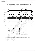


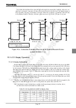
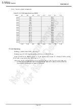
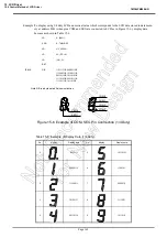
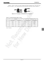

Page 154
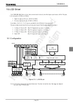
15. LCD Driver
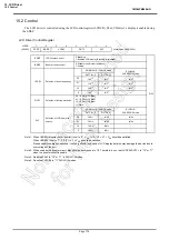
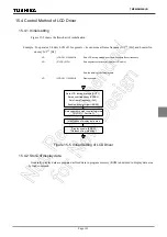
15.2 Control
TMP86PM29BUG
15.2 Control
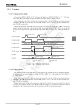
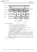
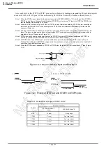
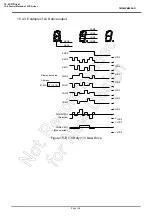
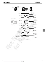
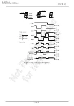
The LCD driver is controlled using the LCD control register (LCDCR). The LCD driver’s display is enabled using
the EDSP.
Note 1: When <BRES>(Booster circuit control) is set to “0”, V
DD
≥
V3
≥
V2
≥
V1
≥
V
SS
should be satisfied.
When <BRES> is set to “1”, 5.5 [V]
≥
V3
≥
V
DD
should be satisfied.
If these conditions are not satisfied, it not only affects the quality of LCD display but also may damage the device due to
over voltage of the port.
Note 2: When used as the booster circuit, bias should be composed to 1/3. Therefore, do not set LCDCR<DUTY> to "10" or "11"
when the booster circuit is enable.
Note 3: Do not set SLF to “10” or “11” in SLOW1/2 modes.
Note 4: Do not set VFSEL to “11” SLOW1/2 modes.
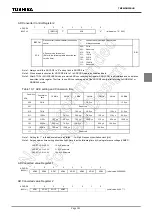
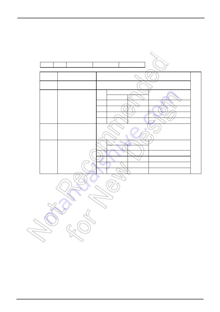
LCD Driver Control Register
LCDCR
(0028H)
7
6
5
4
3
2
1
0
EDSP
BRES
VFSEL
DUTY
SLF
(Initial value: 0000 0000)
EDSP
LCD Display Control
0: Blanking
1: Enables LCD display (Blanking is released)
R/W
BRES
Booster circuit control
0: Disable (use divider resistance)
1: Enable
VFSEL
Selection of boost frequency
NORMAL1/2, IDLE/1/2 mode
SLOW1/2,
SLEEP0/1/2 mode
DV7CK = 0
DV7CK = 1
00
fc/2
13
fs/2
5
fs/2
5
01
fc/2
11
fs/2
3
fs/2
3
10
fc/2
10
fs/2
2
fs/2
2
11
fc/2
9
fc/2
9
–
DUTY
Selection of driving methods
00: 1/4 Duty (1/3 Bias)
01: 1/3 Duty (1/3 Bias)
10: 1/2 Duty (1/2 Bias)
11: Static
SLF
Selection of LCD frame fre-
quency
NORMAL1/2, IDLE/1/2 mode
SLOW1/2,
SLEEP0/1/2 mode
DV7CK = 0
DV7CK = 1
00
fc/2
17
fs/2
9
fs/2
9
01
fc/2
16
fs/28
fs/2
8
10
fc/2
15
fc/2
15
–
11
fc/2
13
fc/2
13
–
Summary of Contents for TLCS-870/C Series
Page 1: ...8 Bit Microcontroller TLCS 870 C Series TMP86PM29BUG ...
Page 6: ...TMP86PM29BUG ...
Page 7: ...Revision History Date Revision 2007 10 11 1 First Release 2008 8 29 2 Contents Revised ...
Page 9: ......
Page 15: ...vi ...
Page 19: ...Page 4 1 3 Block Diagram TMP86PM29BUG 1 3 Block Diagram Figure 1 2 Block Diagram ...
Page 23: ...Page 8 1 4 Pin Names and Functions TMP86PM29BUG ...
Page 48: ...Page 33 TMP86PM29BUG ...
Page 49: ...Page 34 2 Operational Description 2 3 Reset Circuit TMP86PM29BUG ...
Page 61: ...Page 46 3 Interrupt Control Circuit 3 8 External Interrupts TMP86PM29BUG ...
Page 81: ...Page 66 6 Watchdog Timer WDT 6 3 Address Trap TMP86PM29BUG ...
Page 135: ...Page 120 10 8 Bit TimerCounter TC5 TC6 10 1 Configuration TMP86PM29BUG ...
Page 145: ...Page 130 11 Asynchronous Serial interface UART 11 9 Status Flag TMP86PM29BUG ...
Page 165: ...Page 150 13 10 bit AD Converter ADC 13 6 Precautions about AD Converter TMP86PM29BUG ...
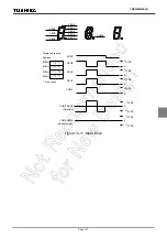
Page 183: ...Page 168 15 LCD Driver 15 4 Control Method of LCD Driver TMP86PM29BUG ...
Page 201: ...Page 186 18 Electrical Characteristics 18 9 Handling Precaution TMP86PM29BUG ...
Page 203: ...Page 188 19 Package Dimensions TMP86PM29BUG ...
Page 205: ......


