

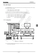


Page 157
TMP86PM29BUG
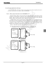
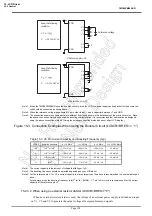
15.2.3 Driving method for LCD driver
In the TMP86PM29BUG, LCD driving voltages can be generated using either an internal booster circuit or
an external resistor divider. This selection is made in LCDCR<BRES>.
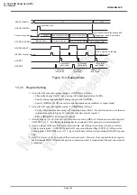
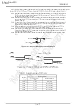
15.2.3.1 When using the booster circuit (LCDCR<BRES>="1")
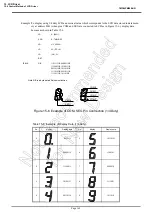
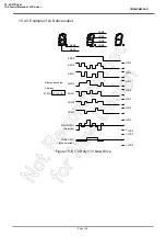
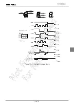
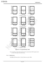
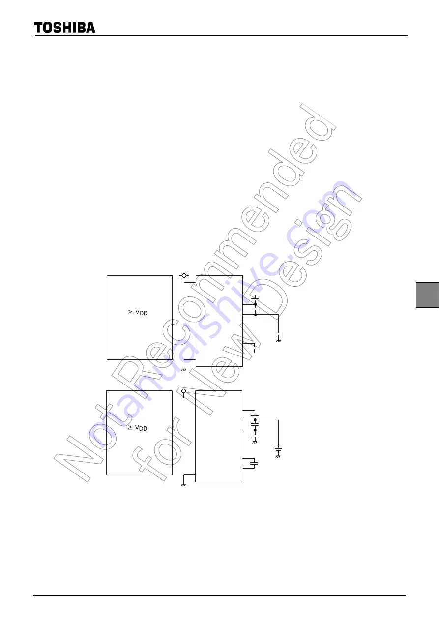
When the reference voltage is connected to the V1 pin, the booster circuit boosts the reference voltage
twofold (V2) or threefold (V3) to generate the output voltages for segment/common signals. When the
reference voltage is connected to the V2 pin, it is reduced to 1/2 (V1) or boosted to 3/2 (V3). When the
reference voltage is connected to the V3 pin, it is reduced to 1/3 (V1) or 2/3 (V2).
LCDCR<VFSEL> is used to select the reference frequency in the booster circuit. The faster the boost-
ing frequency, the higher the segment/common drive capability, but power consumption is increased.
Conversely, the slower the boosting frequency, the lower the segment/common drive capability, but power
consumption is reduced. If the drive capability is insufficient, the LCD may not be displayed clearly.
Therefore, select an optimum boosting frequency for the LCD panel to be used.
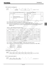
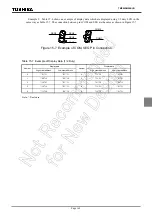
Table 15-3 shows the V3 pin current capacity and boosting frequency.
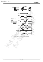
Note: When used as the booster circuit, bias should be composed to 1/3. Therefore, do not set
LCDCR<DUTY> to "10" or "11" when the booster circuit is enable (LCDCR<BRES>="1").
V3
V2
V1
C1
C0
VDD
VSS
Keep the following
condition.
V1 =
V3
Reference voltage
C
C
C
C
= 0.1 to 0.47
µ
F
1/3 x V3
a) Reference pin = V1
V3
V2
V1
C1
C0
VDD
VSS
Keep the following
condition.
V2 =
V3
Reference voltage
C
C
C
C
= 0.1 to 0.47
µ
F
b) Reference pin = V2
C
2/3 x V3
Summary of Contents for TLCS-870/C Series
Page 1: ...8 Bit Microcontroller TLCS 870 C Series TMP86PM29BUG ...
Page 6: ...TMP86PM29BUG ...
Page 7: ...Revision History Date Revision 2007 10 11 1 First Release 2008 8 29 2 Contents Revised ...
Page 9: ......
Page 15: ...vi ...
Page 19: ...Page 4 1 3 Block Diagram TMP86PM29BUG 1 3 Block Diagram Figure 1 2 Block Diagram ...
Page 23: ...Page 8 1 4 Pin Names and Functions TMP86PM29BUG ...
Page 48: ...Page 33 TMP86PM29BUG ...
Page 49: ...Page 34 2 Operational Description 2 3 Reset Circuit TMP86PM29BUG ...
Page 61: ...Page 46 3 Interrupt Control Circuit 3 8 External Interrupts TMP86PM29BUG ...
Page 81: ...Page 66 6 Watchdog Timer WDT 6 3 Address Trap TMP86PM29BUG ...
Page 135: ...Page 120 10 8 Bit TimerCounter TC5 TC6 10 1 Configuration TMP86PM29BUG ...
Page 145: ...Page 130 11 Asynchronous Serial interface UART 11 9 Status Flag TMP86PM29BUG ...
Page 165: ...Page 150 13 10 bit AD Converter ADC 13 6 Precautions about AD Converter TMP86PM29BUG ...
Page 183: ...Page 168 15 LCD Driver 15 4 Control Method of LCD Driver TMP86PM29BUG ...
Page 201: ...Page 186 18 Electrical Characteristics 18 9 Handling Precaution TMP86PM29BUG ...
Page 203: ...Page 188 19 Package Dimensions TMP86PM29BUG ...
Page 205: ......


