

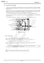
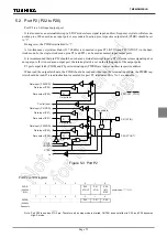

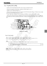

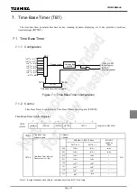
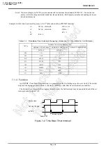

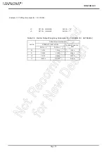
Page 56
5. I/O Ports
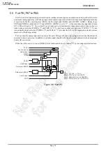
5.5 Port P6 (P67 to P60)
TMP86PM29BUG
5.5
Port P6 (P67 to P60)
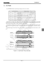
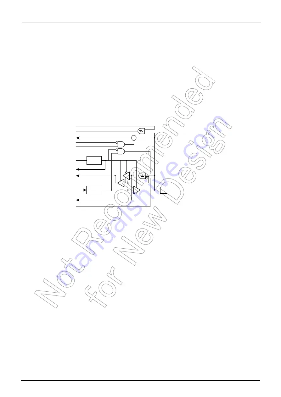
Port P6 is an 8-bit input/output port which can be configured as an input or an output in one-bit unit. Port P6 is also
used as an analog input, Key on Wake up input, timer/counter input and external interrupt input. Input/output modes
is specified by the P6 control register (P6CR), the P6 output latch (P6DR), and ADCCR1<AINDS>. During reset,
P6CR and P6DR are initialized to “0” and ADCCR1<AINDS> is set to “1”. At the same time, the input data of pins
P67 to P60 are fixed to “0”. To use port P6 as an input port, external interrupt input, timer/counter input or key on
wake up input, set data of P6DR to “1” and P6CR to “0”. To use it as an output port, set data of P6CR to “1”. To use
it as an analog input, set data of P6DR to “0” and P6CR to “0”, and start the AD. It is the penetration electric current
measures by the analog voltage.
Pins not used for analog input can be used as I/O ports. During AD conversion, output instructions should not be
executed to keep a precision. In addition, a variable signal should not be input to a port adjacent to the analog input
during AD conversion.
When the AD converter is in use (P6DR=0), bits mentioned above are read as “0” by executing input instructions.
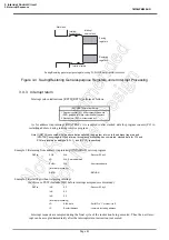
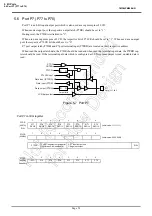
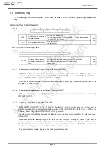
Figure 5-6 Port P6
Data input (P6DR)
Data output (P6DR)
Key on wake up
Analog input
STOPj
STOP
Control input
AINDS
SAIN
P6CRi
P6CRi input
P6i
Note 1: i = 7
to
0, j = 7 to 4
Note 2: STOP is bit 7 in SYSCR1
Note 3: SAIN is bit 0 to 3 in ADCCRA
Note 4: STOPj is bit 4 to 7 in STOPCR.
D Q
D Q
Summary of Contents for TLCS-870/C Series
Page 1: ...8 Bit Microcontroller TLCS 870 C Series TMP86PM29BUG ...
Page 6: ...TMP86PM29BUG ...
Page 7: ...Revision History Date Revision 2007 10 11 1 First Release 2008 8 29 2 Contents Revised ...
Page 9: ......
Page 15: ...vi ...
Page 19: ...Page 4 1 3 Block Diagram TMP86PM29BUG 1 3 Block Diagram Figure 1 2 Block Diagram ...
Page 23: ...Page 8 1 4 Pin Names and Functions TMP86PM29BUG ...
Page 48: ...Page 33 TMP86PM29BUG ...
Page 49: ...Page 34 2 Operational Description 2 3 Reset Circuit TMP86PM29BUG ...
Page 61: ...Page 46 3 Interrupt Control Circuit 3 8 External Interrupts TMP86PM29BUG ...
Page 81: ...Page 66 6 Watchdog Timer WDT 6 3 Address Trap TMP86PM29BUG ...
Page 135: ...Page 120 10 8 Bit TimerCounter TC5 TC6 10 1 Configuration TMP86PM29BUG ...
Page 145: ...Page 130 11 Asynchronous Serial interface UART 11 9 Status Flag TMP86PM29BUG ...
Page 165: ...Page 150 13 10 bit AD Converter ADC 13 6 Precautions about AD Converter TMP86PM29BUG ...
Page 183: ...Page 168 15 LCD Driver 15 4 Control Method of LCD Driver TMP86PM29BUG ...
Page 201: ...Page 186 18 Electrical Characteristics 18 9 Handling Precaution TMP86PM29BUG ...
Page 203: ...Page 188 19 Package Dimensions TMP86PM29BUG ...
Page 205: ......


