Chapter 7 External Bus Controller
7-2
7.2 Block
Diagram
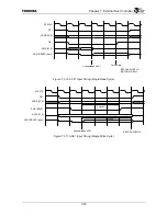
Figure 7.2.1 Block Diagram of External Bus Controller
Boot
Options
CE
*
[5:0]
BWE
*
[3:0]/BE
*
[3:0]
OE
*
G-Bus I/F
G-Bus
ACEHOLD
SYSSP
Register Address
Decoder
Host I/F Timing
Control
Channel Control
Register
Address
Decoder
Channel Control
Register
Address
Decoder
CH0
CH7
Timing
Control
EBIF
SWE
*
ACK
*
/READY
ADDR[19:0]
EBIF Control
UAE
DATA[31:0]
BUSSPRT
*
External Bus Controller (EBUSC)
CG
SYSCLK
CARDREG
*
CARDDIR
*
CARD1CSH/L
*
,CARD2CSH/L
*
CARDIORD
*
CARDIOWR
*
CARD1WAIT
*
,CARD2WAIT
*
Summary of Contents for TMPR4925
Page 1: ...64 Bit TX System RISC TX49 Family TMPR4925 Rev 3 0 ...
Page 4: ......
Page 15: ...Handling Precautions ...
Page 16: ......
Page 18: ...1 Using Toshiba Semiconductors Safely 1 2 ...
Page 40: ...3 General Safety Precautions and Usage Considerations 3 18 ...
Page 42: ...4 Precautions and Usage Considerations 4 2 ...
Page 43: ...TMPR4925 ...
Page 44: ......
Page 54: ...Chapter 1 Features 1 8 ...
Page 58: ...Chapter 2 Block Diagram 2 4 ...
Page 88: ...Chapter 4 Address Mapping 4 12 ...
Page 226: ...Chapter 8 DMA Controller 8 58 ...
Page 260: ...Chapter 9 SDRAM Controller 9 34 ...
Page 480: ...Chapter 15 Interrupt Controller 15 32 ...
Page 554: ...Chapter 19 Real Time Clock RTC 19 8 ...
Page 555: ...Chapter 20 Removed 20 1 20 Removed ...
Page 556: ...Chapter 20 Removed 20 2 ...
Page 564: ...Chapter 21 Extended EJTAG Interface 21 8 ...
Page 580: ...Chapter 22 Electrical Characteristics 22 16 ...
Page 588: ...Chapter 24 Usage Notes 24 2 ...

