Chapter 7 External Bus Controller
7-15
7.3.7.4 ACK
*
Input Timing (External ACK Mode)
The ACK* signal becomes an input signal when in the external ACK mode.
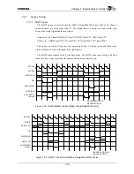
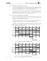
During a Read cycle, data latched timing is selectable from two cases by EBCCRn.LDEA bit.
When EBCCRn.LDEA is zero, data is latched two clock cycles after assertion of the ACK* signal
is acknowledged (Figure 7.3.9 ACK* Input Timing (Single Read Cycle)). When EBCCRn.LDEA
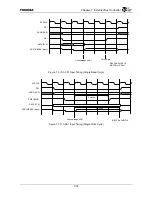
is one, data is latched at the assertion of the ACK* signal is acknowledged (Figure 7.3.10 ACK*
Input Timing (Single Read Cycle)). During a Write cycle, assertion of the ACK* signal is
acknowledged, SWE*/BWE* is deasserted three clock cycles later, then data is held for one clock
cycle after that (Figure 7.3.11 ACK* Input Timing (Single Write Cycle).
The ACK* input signal is internally initialized. Due to internal State Machine restrictions,
ACK* cannot be acknowledged consecutively on consecutive clock cycles. External devices can
assert ACK* across multiple clock cycles under the following conditions.
•
During Single access, the ACK* signal can be asserted before the end of the cycle during
which CE* is dasserted.
•
During Burst access, it is possible to assert the ACK* signal for up to three clock cycles
during Reads and for up to five clock cycles during Writes. If the ACK* signal is asserted for
a period longer than this, it will be acknowledged as the next valid ACK* signal.
Figure 7.3.9 ACK
*
Input Timing (Single Read Cycle)
SYSCLK
CE
*
ADDR [19
:
0]
OE
*
DATA [31
:
0]
ACK
*
/READY (Input)
Latch Data
Acknowledge ACK
*
2 clocks
EBCCRn.SHWT=0
EBCCRn.LDEA=0
Summary of Contents for TMPR4925
Page 1: ...64 Bit TX System RISC TX49 Family TMPR4925 Rev 3 0 ...
Page 4: ......
Page 15: ...Handling Precautions ...
Page 16: ......
Page 18: ...1 Using Toshiba Semiconductors Safely 1 2 ...
Page 40: ...3 General Safety Precautions and Usage Considerations 3 18 ...
Page 42: ...4 Precautions and Usage Considerations 4 2 ...
Page 43: ...TMPR4925 ...
Page 44: ......
Page 54: ...Chapter 1 Features 1 8 ...
Page 58: ...Chapter 2 Block Diagram 2 4 ...
Page 88: ...Chapter 4 Address Mapping 4 12 ...
Page 226: ...Chapter 8 DMA Controller 8 58 ...
Page 260: ...Chapter 9 SDRAM Controller 9 34 ...
Page 480: ...Chapter 15 Interrupt Controller 15 32 ...
Page 554: ...Chapter 19 Real Time Clock RTC 19 8 ...
Page 555: ...Chapter 20 Removed 20 1 20 Removed ...
Page 556: ...Chapter 20 Removed 20 2 ...
Page 564: ...Chapter 21 Extended EJTAG Interface 21 8 ...
Page 580: ...Chapter 22 Electrical Characteristics 22 16 ...
Page 588: ...Chapter 24 Usage Notes 24 2 ...

