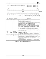
Chapter 8 DMA Controller
8-14
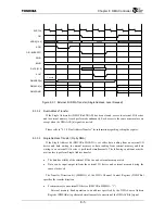
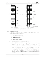
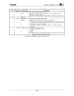
(a) Address offset is equivalent
(b) Address offset differs
Figure 8.3.4 Dual Address Burst Transfer (DMCCRn.USEXFSZ
=
0)
50
54
58
5c
64
68
6c
60
74
78
7c
70
00
04
08
0c
14
18
1c
10
32
0
10
14
18
1c
24
28
2c
20
34
38
3c
30
40
44
48
4c
54
58
5c
50
32
0
Source Address
FIFO (8 Double Words)
Destination Address
50
54
58
5c
64
68
6c
60
74
78
7c
70
00
04
08
1c
14
18
1c
10
32
0
10
14
18
1c
24
28
2c
20
34
38
3c
30
40
44
48
4c
54
58
5c
50
32
0
24
28
2c
20
30
68
6c
70
64
60
Summary of Contents for TMPR4925
Page 1: ...64 Bit TX System RISC TX49 Family TMPR4925 Rev 3 0 ...
Page 4: ......
Page 15: ...Handling Precautions ...
Page 16: ......
Page 18: ...1 Using Toshiba Semiconductors Safely 1 2 ...
Page 40: ...3 General Safety Precautions and Usage Considerations 3 18 ...
Page 42: ...4 Precautions and Usage Considerations 4 2 ...
Page 43: ...TMPR4925 ...
Page 44: ......
Page 54: ...Chapter 1 Features 1 8 ...
Page 58: ...Chapter 2 Block Diagram 2 4 ...
Page 88: ...Chapter 4 Address Mapping 4 12 ...
Page 226: ...Chapter 8 DMA Controller 8 58 ...
Page 260: ...Chapter 9 SDRAM Controller 9 34 ...
Page 480: ...Chapter 15 Interrupt Controller 15 32 ...
Page 554: ...Chapter 19 Real Time Clock RTC 19 8 ...
Page 555: ...Chapter 20 Removed 20 1 20 Removed ...
Page 556: ...Chapter 20 Removed 20 2 ...
Page 564: ...Chapter 21 Extended EJTAG Interface 21 8 ...
Page 580: ...Chapter 22 Electrical Characteristics 22 16 ...
Page 588: ...Chapter 24 Usage Notes 24 2 ...


