Chapter 8 DMA Controller
8-31
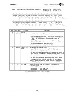
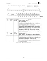
8.4.5
DMA Destination Address Register (DMDARn)
0xB008 (ch. 0) 0xB028 (ch. 1)
0xB048 (ch. 2) 0xB068 (ch. 3)
31
16
DADDR[31:16]
R/W
:
Type
-
: Initial value
15
0
DADDR[15:0]
R/W
:
Type
-
: Initial value
Bits Mnemonic Field
Name
Description
31:0 DADDR
Destination
Address
Destination Address (Initial value: undefined, R/W)
This register sets the physical address of the transfer destination during Dual
Address transfer. This register is ignored during Single Address transfer.
Refer to “8.3.8.1 Channel Register Settings During Dual Address Transfer” for more
information.
During Burst transfer, the value changes only by the size of data transferred during
each single bus operation. During Single transfer, the value only changes by the
value specified by the DMA Destination Address Increment Register (DMDAIRn).
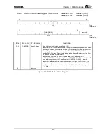
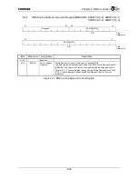
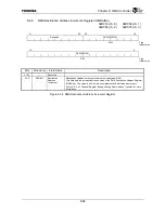
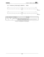
Figure 8.4.5 DMA Destination Address Register
Summary of Contents for TMPR4925
Page 1: ...64 Bit TX System RISC TX49 Family TMPR4925 Rev 3 0 ...
Page 4: ......
Page 15: ...Handling Precautions ...
Page 16: ......
Page 18: ...1 Using Toshiba Semiconductors Safely 1 2 ...
Page 40: ...3 General Safety Precautions and Usage Considerations 3 18 ...
Page 42: ...4 Precautions and Usage Considerations 4 2 ...
Page 43: ...TMPR4925 ...
Page 44: ......
Page 54: ...Chapter 1 Features 1 8 ...
Page 58: ...Chapter 2 Block Diagram 2 4 ...
Page 88: ...Chapter 4 Address Mapping 4 12 ...
Page 226: ...Chapter 8 DMA Controller 8 58 ...
Page 260: ...Chapter 9 SDRAM Controller 9 34 ...
Page 480: ...Chapter 15 Interrupt Controller 15 32 ...
Page 554: ...Chapter 19 Real Time Clock RTC 19 8 ...
Page 555: ...Chapter 20 Removed 20 1 20 Removed ...
Page 556: ...Chapter 20 Removed 20 2 ...
Page 564: ...Chapter 21 Extended EJTAG Interface 21 8 ...
Page 580: ...Chapter 22 Electrical Characteristics 22 16 ...
Page 588: ...Chapter 24 Usage Notes 24 2 ...

