Chapter 8 DMA Controller
8-54
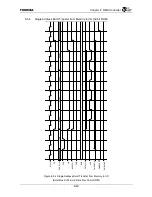
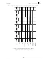
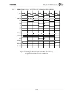
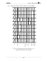
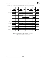
8.5.16 External I/O Device – SDRAM Dual Address Transfer
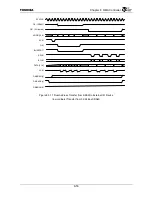
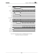
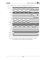
Figure 8.5.18 Dual Address Transfer from External I/O Device to SDRAM
(4-word Burst Transfer to 32-bit SDRAM)
SDCLK/SYSCLK
CE
*
ADDR [19:0]
DQM[7:0]
DATA [31:0]
SWE
*
ACK
*
DMAREQ[n]
DMAACK[n]
DMADONE
*
ACE
*
BWE
*
CS
*
RAS
*
CAS
*
WE
*
CKE
X
X
X
f
V
V
V
V
Valid
V
V
V
ff
f0 ff
OE
*
BUSSPRT
*
Summary of Contents for TMPR4925
Page 1: ...64 Bit TX System RISC TX49 Family TMPR4925 Rev 3 0 ...
Page 4: ......
Page 15: ...Handling Precautions ...
Page 16: ......
Page 18: ...1 Using Toshiba Semiconductors Safely 1 2 ...
Page 40: ...3 General Safety Precautions and Usage Considerations 3 18 ...
Page 42: ...4 Precautions and Usage Considerations 4 2 ...
Page 43: ...TMPR4925 ...
Page 44: ......
Page 54: ...Chapter 1 Features 1 8 ...
Page 58: ...Chapter 2 Block Diagram 2 4 ...
Page 88: ...Chapter 4 Address Mapping 4 12 ...
Page 226: ...Chapter 8 DMA Controller 8 58 ...
Page 260: ...Chapter 9 SDRAM Controller 9 34 ...
Page 480: ...Chapter 15 Interrupt Controller 15 32 ...
Page 554: ...Chapter 19 Real Time Clock RTC 19 8 ...
Page 555: ...Chapter 20 Removed 20 1 20 Removed ...
Page 556: ...Chapter 20 Removed 20 2 ...
Page 564: ...Chapter 21 Extended EJTAG Interface 21 8 ...
Page 580: ...Chapter 22 Electrical Characteristics 22 16 ...
Page 588: ...Chapter 24 Usage Notes 24 2 ...

