Chapter 9 SDRAM Controller
9-7
9.3.2.3
Address Signal Mapping (16-bit Data Bus)
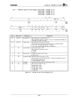
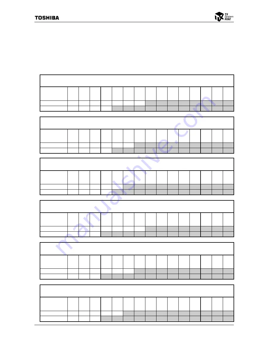
Table 9.3.3 shows the address signal mapping when using a 16-bit data bus. B0 is used in the
bank selection in memory with a two-bank configuration. [B1:B0] are used in the bank selection
in memory with a four-bank configuration. Bits with the description “L/H” output High when
performing auto-precharging, or output Low when not performing auto-precharging.
Table 9.3.3 Address Signal Mapping (16-bit Data Bus) (1/2)
Row Address Width = 11
Column Address Width = 8
Address Bit
ADDR [19:5]
19
(B0)
18
(B1)
17 16
SAD
DR10
(AP)
14 13 12 11 10 9 8 7 6 5
Column
Address
20 21 21 20 L/H 21 20 8
7
6
5
4
3
2
1
Row
Address 20 21 21 20 19
18
17
16
15
14
13
12
11
10
9
Row Address Width
=
11
Column Address Width
=
9
Address Bit
ADDR [19:5]
19
(B0)
18
(B1)
17 16
SAD
DR10
(AP)
14 13 12 11 10 9 8 7 6 5
Column
Address
21 21 21 20 L/H 21 20
8
7
6
5
4
3
2
1
Row
Address 21 21 21 20 19
18
17
16
15
14
13
12
11
10
9
Row Address Width
=
11
Column Address Width
=
10
Address Bit
ADDR [19:5]
19
(B0)
18
(B1)
17 16
SAD
DR10
(AP)
14 13 12 11 10 9 8 7 6 5
Column
Address
22 21 21 20 L/H 21
20
8
7
6
5
4
3
2
1
Row
Address 22 21 21 20 19
18
17
16
15
14
13
12
11
10
9
Row Address Width
=
12
Column Address Width
=
8
Address Bit
ADDR [19:5]
19
(B0)
18
(B1)
17 16
SAD
DR10
(AP)
14 13 12 11 10 9 8 7 6 5
Column
Address
21 22 21 20 L/H 22 21 8
7
6
5
4
3
2
1
Row
Address 21 22 21 20
19
18
17
16
15
14
13
12
11
10
9
Row Address Width
=
12
Column Address Width
=
9
Address Bit
ADDR [19:5]
19
(B0)
18
(B1)
17 16
SAD
DR10
(AP)
14 13 12 11 10 9 8 7 6 5
Column
Address
22 23 21 20 L/H 22 21
8
7
6
5
4
3
2
1
Row
Address 22 23 21 20
19
18
17
16
15
14
13
12
11
10
9
Row Address Width
=
12
Column Address Width
=
10
Address Bit
ADDR [19:5]
19
(B0)
18
(B1)
17 16
SAD
DR10
(AP)
14 13 12 11 10 9 8 7 6 5
Column
Address
23 24 21 20 L/H 22
21
8
7
6
5
4
3
2
1
Row
Address 23 24 21 20
19
18
17
16
15
14
13
12
11
10
9
Summary of Contents for TMPR4925
Page 1: ...64 Bit TX System RISC TX49 Family TMPR4925 Rev 3 0 ...
Page 4: ......
Page 15: ...Handling Precautions ...
Page 16: ......
Page 18: ...1 Using Toshiba Semiconductors Safely 1 2 ...
Page 40: ...3 General Safety Precautions and Usage Considerations 3 18 ...
Page 42: ...4 Precautions and Usage Considerations 4 2 ...
Page 43: ...TMPR4925 ...
Page 44: ......
Page 54: ...Chapter 1 Features 1 8 ...
Page 58: ...Chapter 2 Block Diagram 2 4 ...
Page 88: ...Chapter 4 Address Mapping 4 12 ...
Page 226: ...Chapter 8 DMA Controller 8 58 ...
Page 260: ...Chapter 9 SDRAM Controller 9 34 ...
Page 480: ...Chapter 15 Interrupt Controller 15 32 ...
Page 554: ...Chapter 19 Real Time Clock RTC 19 8 ...
Page 555: ...Chapter 20 Removed 20 1 20 Removed ...
Page 556: ...Chapter 20 Removed 20 2 ...
Page 564: ...Chapter 21 Extended EJTAG Interface 21 8 ...
Page 580: ...Chapter 22 Electrical Characteristics 22 16 ...
Page 588: ...Chapter 24 Usage Notes 24 2 ...

