Chapter 10 PCI Controller
10-6
10.3.3 Supported PCI Bus Commands
Table 10.3.1 shows the PCI Bus commands that the PCI Controller supports.
Table 10.3.1 Supported PCI Bus Commands
C/BE Value
PCI Command
As Initiator
As Target
0000 Interrupt
Acknowledge †
⎯
0001 Special
Cycle †
⎯
0010 I/O
Read
√
√
0011 I/O
Write
√
√
0100 (Reserved)
⎯
⎯
0101 (Reserved)
⎯
⎯
0110 Memory
Read
√
√
0111 Memory
Write
√
√
1000 (Reserved)
⎯
⎯
1001 (Reserved)
⎯
⎯
1010 Configuration
Read
√
‡
1011 Configuration
Write
√
‡
1100 Memory
Read
Multiple
√
√
1101 Dual
Address
Cycle
⎯
⎯
1110
Memory Read Line
√
√
1111
Memory Write and Invalidate
√
√
Note: In the case of I/O read, I/O write, single access memory read and memory write, the
required byte enables are asserted. In the case of burst access memory read, 4-byte
enables are asserted.
√
: Supported when in both the Host mode and the Satellite mode
† : Supported only when in the Host mode
‡ : Supported only when in the Satellite mode
— : Not supported
•
I/O Read, I/O Write, Memory Read, Memory Write
This command executes Read/Write access to the address mapped on the G-Bus and PCI Bus.
•
Memory Read Multiple, Memory Read Line
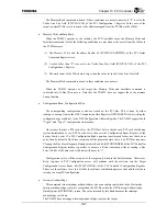
The Memory Read Multiple command is issued if all of the following conditions are met when
the Initiator function is operating and Burst Read access is issued from the G-Bus to the PCI Bus.
(1) A value other than “0” is set to the Cache Line Size Field (PCICFG1.CLS) of the PCI
Configuration 1 Register.
(2) The Read data word count is larger than the value set in the Cache Line Size Field.
Also, the Read Memory Line command is issued when all of the following conditions are met.
(1) A value other than “0” is set to the Cache Line Size Field (PCICFG1.CLS) of the PCI
Configuration 1 Register.
(2) The Read data word count is larger than the value set in the Cache Line Size Field.
Summary of Contents for TMPR4925
Page 1: ...64 Bit TX System RISC TX49 Family TMPR4925 Rev 3 0 ...
Page 4: ......
Page 15: ...Handling Precautions ...
Page 16: ......
Page 18: ...1 Using Toshiba Semiconductors Safely 1 2 ...
Page 40: ...3 General Safety Precautions and Usage Considerations 3 18 ...
Page 42: ...4 Precautions and Usage Considerations 4 2 ...
Page 43: ...TMPR4925 ...
Page 44: ......
Page 54: ...Chapter 1 Features 1 8 ...
Page 58: ...Chapter 2 Block Diagram 2 4 ...
Page 88: ...Chapter 4 Address Mapping 4 12 ...
Page 226: ...Chapter 8 DMA Controller 8 58 ...
Page 260: ...Chapter 9 SDRAM Controller 9 34 ...
Page 480: ...Chapter 15 Interrupt Controller 15 32 ...
Page 554: ...Chapter 19 Real Time Clock RTC 19 8 ...
Page 555: ...Chapter 20 Removed 20 1 20 Removed ...
Page 556: ...Chapter 20 Removed 20 2 ...
Page 564: ...Chapter 21 Extended EJTAG Interface 21 8 ...
Page 580: ...Chapter 22 Electrical Characteristics 22 16 ...
Page 588: ...Chapter 24 Usage Notes 24 2 ...


