3 General Safety Precautions and Usage Considerations
3-9
3.3.10 Decoupling
Spike currents generated during switching can cause Vcc (Vdd) and GND (Vss) voltage levels to fluctuate,
causing ringing in the output waveform or a delay in response speed. (The power supply and GND wiring
impedance is normally 50
Ω
to 100
Ω
.) For this reason, the impedance of power supply lines with respect to
high frequencies must be kept low. This can be accomplished by using thick and short wiring for the Vcc (Vdd)
and GND (Vss) lines and by installing decoupling capacitors (of approximately 0.01
µ
F to 1
µ
F capacitance) as
high-frequency filters between Vcc (Vdd) and GND (Vss) at strategic locations on the printed circuit board.
For low-frequency filtering, it is a good idea to install a 10- to 100-
µ
F capacitor on the printed circuit board (one
capacitor will suffice). If the capacitance is excessively large, however, (e.g. several thousand
µ
F) latch-up can
be a problem. Be sure to choose an appropriate capacitance value.
An important point about wiring is that, in the case of high-speed logic ICs, noise is caused mainly by reflection
and crosstalk, or by the power supply impedance. Reflections cause increased signal delay, ringing, overshoot
and undershoot, thereby reducing the device’s safety margins with respect to noise. To prevent reflections,
reduce the wiring length by increasing the device mounting density so as to lower the inductance (L) and
capacitance (C) in the wiring. Extreme care must be taken, however, when taking this corrective measure, since
it tends to cause crosstalk between the wires. In practice, there must be a trade-off between these two factors.
3.3.11 External
noise
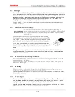
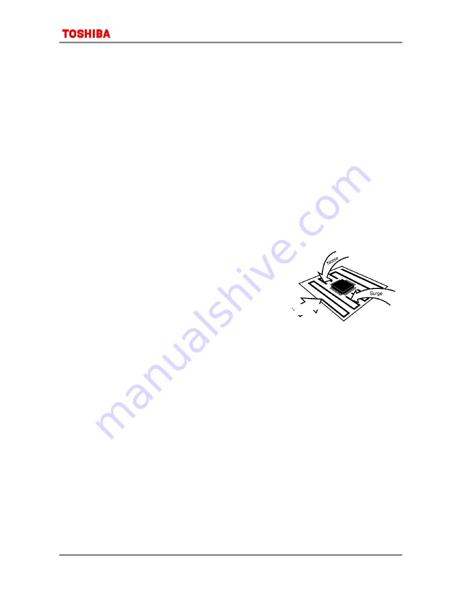
Printed circuit boards with long I/O or signal pattern lines are
vulnerable to induced noise or surges from outside sources.
Consequently, malfunctions or breakdowns can result from overcurrent
or overvoltage, depending on the types of device used. To protect
against noise, lower the impedance of the pattern line or insert a noise-
canceling circuit. Protective measures must also be taken against
surges.
For details of the appropriate protective measures for a particular
device, consult the relevant databook.
3.3.12 Electromagnetic
interference
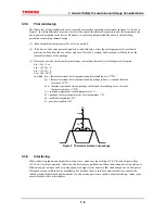
Widespread use of electrical and electronic equipment in recent years has brought with it radio and TV reception
problems due to electromagnetic interference. To use the radio spectrum effectively and to maintain radio
communications quality, each country has formulated regulations limiting the amount of electromagnetic
interference which can be generated by individual products.
Electromagnetic interference includes conduction noise propagated through power supply and telephone lines,
and noise from direct electromagnetic waves radiated by equipment. Different measurement methods and
corrective measures are used to assess and counteract each specific type of noise.
Difficulties in controlling electromagnetic interference derive from the fact that there is no method available
which allows designers to calculate, at the design stage, the strength of the electromagnetic waves which will
emanate from each component in a piece of equipment. For this reason, it is only after the prototype equipment
has been completed that the designer can take measurements using a dedicated instrument to determine the
strength of electromagnetic interference waves. Yet it is possible during system design to incorporate some
measures for the prevention of electromagnetic interference, which can facilitate taking corrective measures
once the design has been completed. These include installing shields and noise filters, and increasing the
thickness of the power supply wiring patterns on the printed circuit board. One effective method, for example, is
to devise several shielding options during design, and then select the most suitable shielding method based on
the results of measurements taken after the prototype has been completed.
Input/Output
Signals
Summary of Contents for TMPR4925
Page 1: ...64 Bit TX System RISC TX49 Family TMPR4925 Rev 3 0 ...
Page 4: ......
Page 15: ...Handling Precautions ...
Page 16: ......
Page 18: ...1 Using Toshiba Semiconductors Safely 1 2 ...
Page 40: ...3 General Safety Precautions and Usage Considerations 3 18 ...
Page 42: ...4 Precautions and Usage Considerations 4 2 ...
Page 43: ...TMPR4925 ...
Page 44: ......
Page 54: ...Chapter 1 Features 1 8 ...
Page 58: ...Chapter 2 Block Diagram 2 4 ...
Page 88: ...Chapter 4 Address Mapping 4 12 ...
Page 226: ...Chapter 8 DMA Controller 8 58 ...
Page 260: ...Chapter 9 SDRAM Controller 9 34 ...
Page 480: ...Chapter 15 Interrupt Controller 15 32 ...
Page 554: ...Chapter 19 Real Time Clock RTC 19 8 ...
Page 555: ...Chapter 20 Removed 20 1 20 Removed ...
Page 556: ...Chapter 20 Removed 20 2 ...
Page 564: ...Chapter 21 Extended EJTAG Interface 21 8 ...
Page 580: ...Chapter 22 Electrical Characteristics 22 16 ...
Page 588: ...Chapter 24 Usage Notes 24 2 ...

