background image

Chapter 10  PCI Controller  


10-67


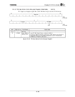
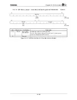
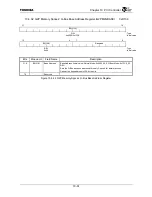
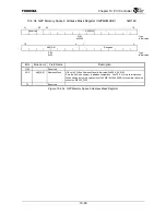
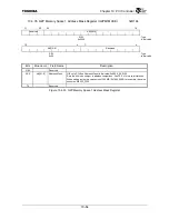
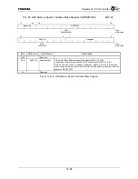
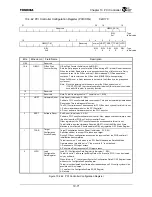
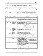
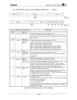
10.4.38  G2P Memory Space 0 PCI Base Address Register (G2PM0PBASE) 

0xD150 


31 


16 

BA[31:16] 


R/W : 

Type 

0x0000 

: Initial value


15 

      8 

7       0 

BA[15:8] Reserved 


R/W  

Type 

0x00 


: Initial value


Bits Mnemonic Field 

Name 

Description 

31:8 

BA[31:8] 

Base Address 

Base Address (Initial value: 0x0000_00, R/W) 

Sets the PCI Base address of Memory Space 0 for initiator access. 

Can set the base address in 256-Byte units. 

7:0 

 Reserved 


Figure 10.4.38  G2P Memory Space 0 PCI Base Address Register 


Summary of Contents for TMPR4925

Page 1: ...64 Bit TX System RISC TX49 Family TMPR4925 Rev 3 0 ...

Page 2: ...e for Semiconductor Devices or TOSHIBA Semiconductor Reliability Handbook etc The Toshiba products listed in this document are intended for usage in general electronics applications computer personal equipment office equipment measuring equipment industrial robotics domestic appliances etc These Toshiba products are neither intended nor warranted for usage in equipment that requires extraordinaril...

Page 3: ...oprocessor a discussion of the application fields in which the microprocessor is utilized and an overview of design methods On the other hand the more experienced designer will find complete technical specifications for this product Toshiba continually updates its technical information Your comments and suggestions concerning this and other Toshiba documents are sincerely appreciated and may be ut...

Page 4: ......

Page 5: ... Extended EJTAG Interface Signals 3 9 3 1 15 Clock Signals 3 10 3 1 16 Initialization Signals 3 10 3 1 17 Test Signals 3 11 3 1 18 Power Supply Pins 3 11 3 2 Boot Configuration 3 12 3 3 Pin Multiplexing 3 15 4 Address Mapping 4 1 4 1 TX4925 Physical Address Map 4 1 4 2 Register Map 4 2 4 2 1 Addressing 4 2 4 2 2 Ways to Access to Internal Registers 4 2 4 2 3 Register Map 4 3 5 Configuration Regist...

Page 6: ... 4 0x9028 ch 5 0x9030 ch 6 0x9038 ch 7 7 28 7 5 Timing Diagrams 7 29 7 5 1 UAE Signal 7 30 7 5 2 Normal Mode Access Single 32 bit Bus 7 32 7 5 3 Normal Mode Access Burst 32 bit Bus 7 36 7 5 4 Normal Mode Access Single 16 bit Bus 7 38 7 5 5 Normal Mode Access Burst 16 bit Bus 7 42 7 5 6 Normal Mode Access Single 8 bit Bus 7 44 7 5 7 Normal Mode Access Burst 8 bit Bus 7 47 7 5 8 Page Mode Access Bur...

Page 7: ...8 5 6 Single Address Single Transfer from Memory to I O 16 bit ROM 8 43 8 5 7 Single Address Single Transfer from I O to Memory 16 bit SRAM 8 44 8 5 8 Single Address Single Transfer from Memory to I O 32 bit Half Speed ROM 8 45 8 5 9 Single Address Single Transfer from I O to Memory 32 bit Half Speed SRAM 8 46 8 5 10 Single Address Single Transfer from Memory to I O 32 bit SRAM 8 47 8 5 11 Single ...

Page 8: ...n ID Register PCICCREV 0xD008 10 29 10 4 4 PCI Configuration 1 Register PCICFG1 0xD00C 10 30 10 4 5 P2G Memory Space 0 PCI Base Address Register P2GM0PBASE 0xD010 10 31 10 4 6 P2G Memory Space 1 PCI Base Address Register P2GM1PBASE 0xD014 10 32 10 4 7 P2G Memory Space 2 PCI Base Address Register P2GM2PBASE 0xD018 10 33 10 4 8 P2G I O Space PCI Base Address Register P2GIOPBASE 0xD01C 10 34 10 4 9 S...

Page 9: ...P2GM1CTR 0xD18C 10 77 10 4 49 P2G Memory Space 2 G Bus Base Address Register P2GM2GBASE 0xD190 10 78 10 4 50 P2G Memory Space 2 Control Register P2GM2CTR 0xD194 10 79 10 4 51 P2G I O Space G Bus Base Address Register P2GIOGBASE 0xD198 10 80 10 4 52 P2G I O Space Control Register P2GIOCTR 0xD19C 10 81 10 4 53 G2P Configuration Address Register G2PCFGADRS 0xD1A0 10 82 10 4 54 G2P Configuration Data ...

Page 10: ...planation 12 3 12 3 1 Overview 12 3 12 3 2 Counter Clock 12 3 12 3 3 Counter 12 4 12 3 4 Interval Timer Mode 12 4 12 3 5 Pulse Generator Mode 12 6 12 3 6 Watchdog Timer Mode 12 7 12 4 Registers 12 9 12 4 1 Timer Control Register n TMTCRn TMTCR0 0xF000 TMTCR1 0xF100 TMTCR2 0xF200 12 10 12 4 2 Timer Interrupt Status Register n TMTISRn TMTISR0 0xF004 TMTISR1 0xF104 TMTISR2 0xF204 12 11 12 4 3 Compare...

Page 11: ... ACDMASEL 0xF784 14 35 14 4 16 ACLC Surround Data Register ACAUDODAT 0xF7A0 ACLC Audio PCM Output Data Register ACSURRDAT 0xF7A4 14 36 14 4 17 ACLC Center Data Register ACCENTDAT 0xF7A8 ACLC LFE Data Register ACLFEDAT 0xF7AC ACLC Audio PCM Input Data Register ACMODODAT 0xF7B8 14 37 14 4 18 ACLC Modem Output Data Register ACAUDIDAT 0xF7B0 14 38 14 4 19 ACLC Modem Input Data Register ACMODIDAT 0xF7B...

Page 12: ... 3 CHI Receive Pointer A Register RXPTRA 0xA808 16 23 16 4 4 CHI Receive Pointer B Register RXPTRB 0xA80C 16 24 16 4 5 CHI Transmit Pointer A Register TXPTRA 0xA810 16 25 16 4 6 CHI Transmit Pointer B Register TXPTRB 0xA814 16 26 16 4 7 CHI SIZE Register CHISIZE 0xA818 16 27 16 4 8 CHI RX Start Register RXSTRT 0xA81C 16 28 16 4 9 CHI TX Start Register TXSTRT 0xA820 16 29 16 4 10 CHI TX Holding Reg...

Page 13: ... 4 1 RTC Register High RTCHI 0xF900 19 4 19 4 2 RTC Register Low RTCLO 0xF904 19 4 19 4 3 Alarm Register High ALARMHI 0xF908 19 5 19 4 4 Alarm Register Low ALARMLO 0xF90C 19 5 19 4 5 RTC Control Register RTCCTRL 0xF910 19 6 19 4 6 RTC Interrupt Status Register RTCINT 0xF914 19 7 20 Removed 20 1 21 Extended EJTAG Interface 21 1 21 1 Extended EJTAG Interface 21 1 21 2 JTAG Boundary Scan Test 21 2 21...

Page 14: ...NAND Flash Memory Interface AC Characteristics 22 13 22 5 13 CHI Interface AC Characteristics 22 14 22 5 14 SPI Interface AC Characteristics 22 15 23 Pin Layout Package 23 1 23 1 Pin Layout 23 1 23 2 Package 23 6 24 Usage Notes 24 1 24 1 Limitation on DMA Data Chaining 24 1 24 2 Limitation on a Register Read After an SIO Software Reset 24 1 24 3 Other Precautions 24 1 Appendix A TX49 H2 Core Suppl...

Page 15: ...Handling Precautions ...

Page 16: ......

Page 17: ... specifications Also please keep in mind the precautions and conditions set forth in the TOSHIBA Semiconductor Reliability Handbook The TOSHIBA products listed in this document are intended for usage in general electronics applications computer personal equipment office equipment measuring equipment industrial robotics domestic appliances etc These TOSHIBA products are neither intended nor warrant...

Page 18: ...1 Using Toshiba Semiconductors Safely 1 2 ...

Page 19: ...you move on to the detailed descriptions of the precautions Explanation of labels Indicates an imminently hazardous situation which will result in death or serious injury if you do not follow instructions Indicates a potentially hazardous situation which could result in death or serious injury if you do not follow instructions Indicates a potentially hazardous situation which if not avoided may re...

Page 20: ... a device is on do not touch the device s heat sink Heat sinks become hot so you may burn your hand Do not touch the tips of device leads Because some types of device have leads with pointed tips you may prick your finger When conducting any kind of evaluation inspection or testing be sure to connect the testing equipment s electrodes or probes to the pins of the device under test before powering ...

Page 21: ...t circuit current will flow continuously and the device may break down or burst into flames resulting in fire or injury When incorporating a visible semiconductor laser into a design use the device s internal photodetector or a separate photodetector to stabilize the laser s radiant power so as to ensure that laser beams exceeding the laser s rated radiant power cannot be emitted If this stabilizi...

Page 22: ...ember to take the device s forward and reverse losses into account The leakage current in these devices is greater than that in ordinary rectifiers as a result if a high speed rectifier is used in an extreme environment e g at high temperature or high voltage its reverse loss may increase causing thermal runaway to occur This may in turn cause the device to explode and scatter shrapnel resulting i...

Page 23: ...ls in the working area are grounded to earth Place a conductive mat over the floor of the work area or take other appropriate measures so that the floor surface is protected against static electricity and is grounded to earth The surface resistivity should be 104 to 108 Ω sq and the resistance between surface and ground 7 5 105 to 108 Ω Cover the workbench surface also with a conductive mat with a...

Page 24: ...rs boxes jigs or bags that are made of anti static materials or materials which dissipate electrostatic charge Make sure that cart surfaces which come into contact with device packaging are made of materials which will conduct static electricity and verify that they are grounded to the floor surface via a grounding chain In any location where the level of static electricity is to be closely contro...

Page 25: ...es and packaging materials with care To avoid damage to devices do not toss or drop packages Ensure that devices are not subjected to mechanical vibration or shock during transportation Ceramic package devices and devices in canister type packages which have empty space inside them are subject to damage from vibration and shock because the bonding wires are secured only at their ends Plastic molde...

Page 26: ... If devices have been stored for more than two years their electrical characteristics should be tested and their leads should be tested for ease of soldering before they are used 3 2 2 Moisture proof packing Moisture proof packing should be handled with care The handling procedure specified for each packing type should be followed scrupulously If the proper procedures are not followed the quality ...

Page 27: ...mperature which it can withstand bake at 125 C for 20 hours Some devices require a different procedure Tube Transfer devices to trays bearing the Heatproof marking or indicating the temperature which they can withstand or to aluminum tubes before baking at 125 C for 20 hours Tape Deviced packed on tape cannot be baked and must be used within the effective usage period after unpacking as specified ...

Page 28: ...ge or current on any pin exceeds the absolute maximum rating the device s internal circuitry can become degraded In the worst case heat generated in internal circuitry can fuse wiring or cause the semiconductor chip to break down If storage or operating temperatures exceed rated values the package seal can deteriorate or the wires can become disconnected due to the differences between the thermal ...

Page 29: ...ss voltage may have been applied only for an instant the large current continues to flow between Vcc Vdd and GND Vss This causes the device to heat up and in extreme cases to emit gas fumes as well To avoid this problem observe the following precautions 1 Do not allow voltage levels on the input and output pins either to rise above Vcc Vdd or to fall below GND Vss Also follow any prescribed power ...

Page 30: ... θca Tc Ta P in which θja thermal resistance between junction and surrounding air C W θjc thermal resistance between junction and package surface or internal thermal resistance C W θca thermal resistance between package surface and surrounding air or external thermal resistance C W Tj junction temperature or chip temperature C Tc package surface temperature or case temperature C Ta ambient tempera...

Page 31: ...g on the types of device used To protect against noise lower the impedance of the pattern line or insert a noise canceling circuit Protective measures must also be taken against surges For details of the appropriate protective measures for a particular device consult the relevant databook 3 3 12 Electromagnetic interference Widespread use of electrical and electronic equipment in recent years has ...

Page 32: ...device insulation Such requirements must be fully taken into account to ensure that your design conforms to the applicable safety standards 3 3 15 Other precautions 1 When designing a system be sure to incorporate fail safe and other appropriate measures according to the intended purpose of your system Also be sure to debug your system under actual board mounted conditions 2 If a plastic package d...

Page 33: ... are essentially two main types of semiconductor device package lead insertion and surface mount During mounting on printed circuit boards devices can become contaminated by flux or damaged by thermal stress from the soldering process With surface mount devices in particular the most significant problem is thermal stress from solder reflow when the entire package is subjected to heat This section ...

Page 34: ...rcuit board use sockets which match the inserted device s package 2 Use sockets whose contacts have the appropriate contact pressure If the contact pressure is insufficient the socket may not make a perfect contact when the device is repeatedly inserted and removed if the pressure is excessively high the device leads may be bent or damaged when they are inserted into or removed from the socket 3 W...

Page 35: ... reflow 3 Using hot air reflow Complete hot air reflow from 30 to 50 seconds at a package surface temperature of between 230 C and 260 C For an example of a recommended temperature profile refer to Figure 4 above 3 5 4 Flux cleaning and ultrasonic cleaning 1 When cleaning circuit boards to remove flux make sure that no residual reactive ions such as Na or Cl remain Note that organic solvents react...

Page 36: ...containing residual chlorine when power to the device is on may cause between lead leakage or migration Therefore Toshiba recommends that these devices be cleaned However if the flux used contains only a small amount of halogen 0 05W or less the devices may be used without cleaning without any problems No cleaning is recommended for TX4925 3 5 6 Mounting tape carrier packages TCPs 1 When tape carr...

Page 37: ...fore doing so you must carefully consider the possible stress and contamination effects that may result and then choose the coating resin which results in the minimum level of stress to the device 3 5 9 Heat sinks 1 When attaching a heat sink to a device be careful not to apply excessive force to the device in the process 2 When attaching a device to a heat sink by fixing it at two or more locatio...

Page 38: ...ity Resin molded devices are sometimes improperly sealed When these devices are used for an extended period of time in a high humidity environment moisture can penetrate into the device and cause chip degradation or malfunction Furthermore when devices are mounted on a regular printed circuit board the impedance between wiring components can decrease under high humidity conditions In systems which...

Page 39: ... the internal chip is exposed When designing circuits make sure that devices are protected against incident light from external sources This problem is not limited to optical semiconductors and EPROMs All types of device can be affected by light 3 6 7 Dust and oil Just like corrosive gases dust and oil can cause chemical reactions in devices which will adversely affect a device s electrical charac...

Page 40: ...3 General Safety Precautions and Usage Considerations 3 18 ...

Page 41: ...se with Toshiba products in microcontroller oscillator applications are listed in Toshiba databooks along with information about oscillation conditions If you use a resonator not included in this list please consult Toshiba or the resonator manufacturer concerning the suitability of the device for your application 2 Undefined functions In some microcontrollers certain instruction code values do no...

Page 42: ...4 Precautions and Usage Considerations 4 2 ...

Page 43: ...TMPR4925 ...

Page 44: ......

Page 45: ...defined R W Read Write is possible W1C Write 1 Clear This corresponding bit is cleared when 1 is written to this bit 0 is invalid if written R W1C Read Write 1 Clear These bits can be read from and written to The corresponding bit is cleared when 1 is written to this bit 0 is invalid if written R W0C Read Write 0 Clear These bits can be read from and written to The corresponding bit is cleared whe...

Page 46: ... described as a diagnostic function is used to facilitate operation evaluations The operation of such functions is not guaranteed References 64 bit TX System RISC TX49 H2 Core Architecture User s Manual http www semicon toshiba co jp eng index html MIPS RISC Architecture Gerry Kane and Joe Heinrich ISBN 0 13 590472 2 See MIPS Run Dominic Sweetman ISBN 1 55860 410 3 MIPS Publications http www mips ...

Page 47: ...n the architecture of the TX49 H2 core including the instruction set refer to the manual 64 bit TX System RISC TX49 H2 Core Architecture The TX4925 is a highly integrated device with integrated peripherals such as SDRAM memory controller NAND Flash memory controller PCI controller AC Link controller PIO SIO SPI CHI PCMCIA I F and Timer This class of product is targeted for applications that requir...

Page 48: ...with the 1 5 V core and the 3 3 V I O while supporting a low power Halt mode CPU maximum operating frequency 200 MHz IEEE1149 1 JTAG support Debug Support Unit Enhanced JTAG 256 pin PBGA package 1 2 1 TX49 H2 Processor Core Features The TX49 H2 is a high performance 64 bit microprocessor core developed by Toshiba 64 bit operation 32 64 bit integer general purpose registers 32 bit physical address ...

Page 49: ...y sizes of 1M byte to 1G byte for devices with 32 bit data bus 1M byte to 512M bytes for devices with 16 bit data bus and 1M byte to 256M bytes for devices with 8 bit data bus 1 2 2 2 DMA Controller DMAC The TX4925 contains a 4 channel DMA controller that executes DMA transfer to memory and I O devices 4 channel independently handling internal external DMA requests Usable 2 channels by external DM...

Page 50: ... and pre charge power down 1 2 2 4 PCI Controller PCIC The TX4925 contains a PCI Controller that complies with PCI Local Bus Specification Revision 2 2 Compliance with PCI Local Bus Specification Revision 2 2 Partly supports power management as optional function 32 bit PCI interface featuring maximum PCI bus clock frequency of 33 MHz Supports both target and initiator functions Supports change of ...

Page 51: ... Surround Center and LFE channels Support Variable Rate Audio recording Playback Support Modem CODEC Line 1 and GPIO slots Support AC link low power mode wake up and warm reset Support sample data I O via DMA transfer 1 2 2 9 Interrupt Controller IRC Interrupt controller in TX4925 supports both internal and external interrupts to the processor core The priority or the value of each interrupt sourc...

Page 52: ...lash memory Controller Controlled NAND Flash I F by Setting Register Supports On chip ECC Error Correct Circuit calculating circuits 1 2 2 13 PCMCIA Interface PCMCIAI F The TX4925 has a 2 identical full PCMCIA ports Provide the control signals and accepts the status signals which conform to the PCMCIA version 2 1 standard Appropriate connector keying and level shifting buffers required for 3 3 V v...

Page 53: ... complies with IEEE1149 1 and real time debugging using a debug support unit DSU built into the TX49 H2 core IEEE 1149 1 JTAG Boundary Scan Real time debugging functions using special emulation probe execution control execution break step and register memory access and PC trace MIPS is the registered trademark of MIPS Technologies Inc SyncFlash is a registered trademark of Micron Technology Inc ...

Page 54: ...Chapter 1 Features 1 8 ...

Page 55: ...ID_SEL DEVSEL REQ 3 2 REQ 1 INTOUT REQ 0 GNT 3 0 PERR SERR CHIFS CHICLK CHIDOUT CHIDIN SCAN_ENB ND_ALE ND_CLE ND_CE ND_RE ND_WE ND_R B TCK TDI DINT TDO TPC 0 TPC 3 1 TMS TRST DCLK PCST 8 0 WBU DSU TX49 H2 Core I Cache D Cache G Bus I F FPU CPU core ACK READY SWE CE 5 0 OE BUSSPRT SDCLK 1 0 RAS CAS SDCS 3 0 DQM 3 0 WE CKE SDCLKIN DATA 31 0 ADDR 19 0 RP SADDR10 UAE SYSCLK CARD2CSL CARD1CSL CARDREG C...

Page 56: ...ovides 6 channels programmable Chip Selects Supports ROMs page mode ROM mask ROM EPROM and EEPROM SRAMs flash ROMs and I O devices 3 DMAC Direct Memory Access Controller Supports transfers to and from both memory and internal external I O devices 4 SDRAMC SDRAM Controller Supports 4 channels 80 MHz bus frequencies 16 or 32 bus width 5 PCIC PCI bus Controller Compliance with PCI Local Bus Specifica...

Page 57: ... bit external data bus and SDRAMC EBUSC 16 CG Clock Generator Incorporates an phase locked loop PLL circuit to drive the multiplied clocks Generates the clocks for each module 17 G Bus High speed bus which is 32 bit bus width within TX4925 Direct connect to TX49 H2 core block 18 IM Bus Low speed bus which is 32 bit bus width within TX4925 Connect to G Bus via IMB 19 IMB G Bus and IM Bus bridge 20 ...

Page 58: ...Chapter 2 Block Diagram 2 4 ...

Page 59: ... ADDR signals are also used as boot configuration signals input during a reset For details of configuration signals refer to Section 3 2 Boot Configuration The ADDR signals are input signals only when the RESET signal is asserted and become output signals after the RESET signal is deasserted Input SADDR10 Input output PU Address10 for SDRAM Address signal for SDRAM refer to Sections 9 3 2 2 and 9 ...

Page 60: ...DRAM controller input signals Input CKE Output Clock Enable CKE signal for SDRAM SyncFlash High SDCS 3 0 Output Synchronous Memory Device Chip Select Chip select signals for SDRAM SyncFlash All High RAS Output Row Address Strobe RAS signal for SDRAM SyncFlash High CAS Output Column Address Strobe CAS signal for SDRAM SyncFlash High WE Output Write Enable WR signal for SDRAM SyncFlash High DQM 3 0 ...

Page 61: ... It becomes an output signal once the RESET signal has been deasserted Input CE 5 4 Output PU Chip Enable Chip select signals for ROM SRAM and I O devices The pins are shared with other functions refer to Section 3 3 Pin Multiplexing All High CE 3 0 Output Chip Enable Chip select signals for ROM SRAM and I O devices All High OE Output Output Enable Output enable signal for ROM SRAM and I O devices...

Page 62: ...A card The pin is shared with other functions refer to Section 3 3 Pin Multiplexing PIO input CARDIOWR Output PU PCMCIA card I O write IOWR signal for a PCMCIA card The pin is shared with other functions refer to Section 3 3 Pin Multiplexing PIO input CARDDIR Output PU PCMCIA card directory Controls the direction of the bidirectional buffer used for a PCMCIA slot This signal is asserted during a r...

Page 63: ...e field of the pin configuration register PCFG PCICLKEN 2 1 Selected by ADDR 18 H High L L PCICLKIO Input output PCI Feedback Clock PCI feedback clock input A boot configuration signal ADDR 18 can determine whether the clock internally generated in the TX4925 is used as PCICLK If the TX4925 internal clock is selected the clock signals are output and simultaneously fed back to the internal PCI bloc...

Page 64: ...ster to request bus mastership The boot configuration signal on the ADDR 1 pin determines whether the built in PCI bus arbiter is used In internal arbiter mode this signal is a PCI bus request input signal In external arbiter mode this signal is a PCI bus request output signal Selected by ADDR 1 H Input L High GNT 3 0 Input output Grant Indicates that bus mastership has been granted to the PCI bus...

Page 65: ...lled up for channel 0 only No pull up resistor is provided for channel 1 3 1 7 Timer Interface Signals Table 3 1 7 Timer Interface Signals Signal Name Type Description Initial State TIMER 1 0 Output PU Timer Output Timer output signals The pins are shared with other functions refer to Section 3 3 Pin Multiplexing PIO input TCLK Input PU External Timer Clock Timer input clock signal TMR0 TMR1 and T...

Page 66: ...he pins are shared with other functions refer to Section 3 3 Pin Multiplexing PIO input 3 1 11 CHI Interface Signals Table 3 1 11 CHI Interface Signals Signal Name Type Description Initial State CHIFS Input output PU CHI Frame synchronization CHI frame synchronization signal This pin can be used in either output or input mode In output mode the pin allows the TX4925 to become the master CHI synchr...

Page 67: ...other functions refer to Section 3 3 Pin Multiplexing PIO input ND_RE Output NAND Flash Read Enable RE signal for NAND flash memory The pin is shared with other functions refer to Section 3 3 Pin Multiplexing PIO input ND_WE Output NAND Flash Write Enable WE signal for NAND flash memory The pin is shared with other functions refer to Section 3 3 Pin Multiplexing PIO input ND_R B Input NAND Flash R...

Page 68: ... pin is shared with other functions refer to Section 3 3 Pin Multiplexing Selected by TDO H PIO input L Low PCST 8 0 Output PC Trace Status Information Outputs PC trace status and other information The pins are shared with other functions refer to Section 3 3 Pin Multiplexing Selected by TDO H PIO input PCST 8 1 BC32K PC ST 0 L All Low 3 1 15 Clock Signals Table 3 1 15 Clock Signals Signal Name Ty...

Page 69: ...igh Input 3 1 18 Power Supply Pins Table 3 1 18 Power Supply Pins Signal Name Type Description Initial State PLL1VDD_A PLL Power Pins PLL analog power supply pins PLL1VDD_A 1 5 V PLL1VSS_A PLL Ground Pins PLL analog ground pins PLL1VSS_A 0 V VccInt VDDC Internal Power Pins Digital power supply pins for internal logic VccInt 1 5 V VccIO VDDS I O Power Pins Digital power supply pins for input output...

Page 70: ... not be pulled down Table 3 2 1 lists the functions that can be set using configuration signals Table 3 2 2 and 3 2 3 describe each configuration signal Note that the functions of some pins vary with the boot memory device used Table 3 2 1 Functions that Can be Set Using Configuration Signals Peripheral Function Functions that Can be Set Configuration Signal PCICLK enable ADDR 18 PCI controller op...

Page 71: ... 18 ADDR 17 CCFG bit 27 ADDR 16 PON deassert edge ADDR 15 PCI Controller Mode Select Specifies the operating mode of the TX4925 PCI controller L Satellite H Host CCFG PCIMODE RESET deassert edge ADDR 14 TX4925 Endian Mode Specifies the TX4925 endian mode L Little endian H Big endian CCFG ENDIAN RESET deassert edge ADDR 13 12 Boot ROM Bus Width Specifies the data bus width when booting from a memor...

Page 72: ...frequency 4 LH 3 SYSCLK frequency GBUSCLK frequency 3 HL 2 SYSCLK frequency GBUSCLK frequency 2 HH 1 SYSCLK frequency GBUSCLK frequency CCFG SYSSP PON deassert edge ADDR 2 Reserved This signal will not be set to 0 upon booting RESET deassert edge ADDR 1 PCI Arbiter Select Selects a PCI bus arbiter L External PCI bus arbiter H Built in PCI bus arbiter CCFG PCIARB RESET deassert edge ADDR 0 TX49 H2 ...

Page 73: ...S 1 INT 5 1 Y16 PIO 14 PIO 14 AC_SYNC ND_RE CTS 1 INT 4 1 V15 PIO 13 PIO 13 AC_SDIN 1 ND_ALE Y15 PIO 12 PIO 12 AC_RST ND_CE Y13 PIO 11 PIO 11 TXD 0 W13 PIO 10 PIO 10 RXD 0 W14 PIO 9 PIO 9 RTS 0 INT 3 1 Y14 PIO 8 PIO 8 CTS 0 INT 2 1 U15 PIO 7 PIO 7 INT 1 1 U13 PIO 6 PIO 6 INT 0 1 V13 PIO 5 PIO 5 SCLK 3 W11 PIO 4 PIO 4 DMAACK 1 W12 PIO 3 PIO 3 DMAREQ 1 V10 PIO 2 PIO 2 DMAACK 0 V12 PIO 1 PIO 1 DMAREQ...

Page 74: ... CE 5 1 0 1 PIO 29 PIO 29 1 0 0 PCST 7 0 CARD2CSL 1 1 CE 4 1 0 1 PIO 28 PIO 28 1 0 0 PCST 5 0 CHIDOUT 1 1 CARD2WAIT 1 1 0 PIO 27 PIO 27 1 0 0 DCLK 0 CARD1CSH 1 1 PIO 26 PIO 26 1 0 TPC 3 0 CARD1CSL 1 1 PIO 25 PIO 25 1 0 TPC 1 0 CARD1WAIT 1 1 PIO 24 PIO 24 1 0 Table 3 3 3 Function Selection for PIO 23 21 2 PCFG Control Bits Pin Name Function Boot Signal TDO SELSPI PCST 2 0 SPICLK 1 1 PIO 23 PIO 23 1...

Page 75: ... 0 PIO 18 CHIDIN 1 Table 3 3 5 Function Selection for PIO 17 12 4 PCFG Control Bits Pin Name Function Boot Signal TDO SELACLC SELNAND SELSIO 1 SELSIOC 1 PIO 17 0 0 0 TXD 1 0 0 1 ND_WE 0 1 PIO 17 AC_SDIN0 1 PIO 16 0 0 0 RXD 1 0 0 1 ND_RB 0 1 PIO 16 AC_SDOUT 1 PIO 15 0 0 0 RTS 1 0 0 1 1 ND_CLE 0 1 PIO 15 AC_BITCLK 1 PIO 14 0 0 0 CTS 1 0 0 1 1 ND_RE 0 1 PIO 14 AC_SYNC 1 PIO 13 0 0 ND_ALE 0 1 PIO 13 A...

Page 76: ...tion Selection for PIO 7 5 6 Pin Name Function Boot Signal TDO PIO 7 PIO 7 1 INT 1 PIO 6 PIO 6 1 INT 0 PIO 5 PIO 5 1 SCLK 1 PIO 7 5 Refer to 2 of Table 3 3 1 Multiplexed Pins Table 3 3 8 Function Selection for PIO 4 0 and BC32K 7 PCFG Control Bits Pin Name Function Boot Signal TDO SELDMA 1 SELDMA 0 SELDONE PIO 4 0 PIO 4 DMAACK 1 1 PIO 3 0 PIO 3 DMAREQ 1 1 PIO 2 0 PIO 2 DMAACK 0 1 PIO 1 0 PIO 1 DMA...

Page 77: ...er setup Refer to the explanation of each controller for the details of the mapping At initialization only the internal registers and the memory space which stores the TX49 H2 core reset vectors are allocated shown as Figure 4 1 1 Usually ROM connected to the external bus controller channel 0 is used for the memory device that stores the reset vectors TX4925 also supports using the memories on PCI...

Page 78: ...re 4 2 1 Generating Physical Address for a Internal Register 4 2 2 Ways to Access to Internal Registers 2 ways to access to the internal registers of TX4925 are supported First is 32 bit register access Second is PCI configuration register access in PCI satellite mode 32 bit register supports 32 bit size access only Another size access without 32 bit size is undefined When the build in PCI control...

Page 79: ... 9 4 0x9000 to 0x9FFF EBUSC Refer to 7 4 0xA000 to 0xA7FF Reserved 0xA800 to 0xAFFF CHI Refer to 16 4 0xB000 to 0xBFFF DMAC Refer to 8 4 0xC000 to 0xCFFF NDFMC Refer to 18 4 0xD000 to 0xDFFF PCIC Refer to 10 4 0xE000 to 0xEFFF CONFIG Refer to 5 2 0xF000 to 0xF0FF TMR0 Refer to 12 4 0xF100 to 0xF1FF TMR1 Refer to 12 4 0xF200 to 0xF2FF TMR2 Refer to 12 4 0xF300 to 0xF3FF SIO0 Refer to 11 4 0xF400 to...

Page 80: ...x901C 32 EBBAR3 EBUS Base Address Register 3 0x9020 32 EBCCR4 EBUS Channel Control Register 4 0x9024 32 EBBAR4 EBUS Base Address Register 4 0x9028 32 EBCCR5 EBUS Channel Control Register 5 0x902c 32 EBBAR5 EBUS Base Address Register 5 0x9030 32 EBCCR6 EBUS Channel Control Register 6 0x9034 32 EBBAR6 EBUS Base Address Register 6 0x9038 32 EBCCR7 EBUS Channel Control Register 7 0x903c 32 EBBAR7 EBUS...

Page 81: ...tination Address Register 2 0xB04C 32 DMCNTR2 DMA Count Register 2 0xB050 32 DMSAIR2 DMA Source Address Increment Register 2 0xB054 32 DMDAIR2 DMA Destination Address Increment Register 2 0xB058 32 DMCCR2 DMA Channel Control Register 2 0xB05C 32 DMCSR2 DMA Channel Status Register 2 0xB060 32 DMCHAR3 DMA Chain Address Register 3 0xB064 32 DMSAR3 DMA Source Address Register 3 0xB068 32 DMDAR3 DMA De...

Page 82: ...0 32 G2PTOCNT G2P Timeout Count register Retry Timeout Value TRDY Timeout Value 0xD060 32 G2PCFG G2P Configuration Register 0xD064 32 G2PSTATUS G2P Status Register 0xD068 32 G2PMASK G2P Interrupt Mask Register 0xD088 32 PCISSTATUS Satellite Mode PCI Status Register Status PMCSR 0xD08C 32 PCIMASK PCI Status Interrupt Mask Register 0xD090 32 P2GCFG P2G Configuration Register 0xD094 32 P2GSTATUS P2G ...

Page 83: ... Address Register 0xD184 32 P2GM0CTR P2G Memory Space 0 G Bus Control Register 0xD188 32 P2GM1GBASE P2G Memory Space 1 G Bus Base Address Register 0xD18C 32 P2GM1CTR P2G Memory Space 1 G Bus Control Register 0xD190 32 P2GM2GBASE P2G Memory Space 2 G Bus Base Address Register 0xD194 32 P2GM2CTR P2G Memory Space 2 G Bus Control Register 0xD198 32 P2GIOGBASE P2G I O Space 0 G Bus Base Address Registe...

Page 84: ...ster 0 0xF008 32 TMCPRA0 Compare Address Register A 0 0xF00C 32 TMCPRB0 Compare Address Register B 0 0xF010 32 TMITMR0 Interval Timer Mode Register 0 0xF020 32 TMCCDR0 Divider Register 0 0xF030 32 TMPGMR0 Plus Generator Mode Register 0 0xF0F0 32 TMTRR0 Timer Read Register 0 Timer Channel 1 0xF100 32 TMTCR1 Timer Control Register 1 0xF104 32 TMTISR1 Timer Interrupt Status Register 1 0xF108 32 TMCPR...

Page 85: ...FO0 Transmitter FIFO Register 0 0xF320 32 SIRFIFO0 Receiver FIFO Register 0 Serial I O Channel 1 0xF400 32 SILCR1 Line Control Register 1 0xF404 32 SIDICR1 DMA Interrupt Control Register 1 0xF408 32 SIDISR1 DMA Interrupt Status Register 1 0xF40C 32 SISCISR1 Status Change Interrupt Status Register 1 0xF410 32 SIFCR1 FIFO Control Register 1 0xF414 32 SIFLCR1 Flow Control Register 1 0xF418 32 SIBGR1 ...

Page 86: ...DEN Interrupt Detection Enable Register 0xF604 32 IRDM0 Interrupt Detection Mode Register 0 0xF608 32 IRDM1 Interrupt Detection Mode Register 1 0xF610 32 IRLVL0 Interrupt Level Register 0 0xF614 32 IRLVL1 Interrupt Level Register 1 0xF618 32 IRLVL2 Interrupt Level Register 2 0xF61C 32 IRLVL3 Interrupt Level Register 3 0xF620 32 IRLVL4 Interrupt Level Register 4 0xF624 32 IRLVL5 Interrupt Level Reg...

Page 87: ...ACLC DMA Request Status Register 0xF784 32 ACDMASEL ACLC DMA Channel Selection Register 0xF7A0 32 ACAUDODAT ACLC Audio PCM Output Data Register 0xF7A4 32 ACSURRDAT ACLC Surround Data Register 0xF7A8 32 ACCENTDAT ACLC Center Data register 0xF7AC 32 ACLFEDAT ACLC LFE Data Register 0xF7B0 32 ACAUDIDAT ACLC Audio PCM Input Data Register 0xF7B8 32 ACMODODAT ACLC Modem Output Data Register 0xF7BC 32 ACM...

Page 88: ...Chapter 4 Address Mapping 4 12 ...

Page 89: ...on register enables the G Bus timeout detection function If a bus response does not occur within the G Bus clock GBUSCLK cycle specified in the G Bus Timeout count register TOCNT the G Bus timeout detection function makes an error response to force the bus access to end The accessed address is stored to the timeout error access address register TOEA If a timeout error is detected while the TX49 H2...

Page 90: ...er 5 2 4 0xE00C 32 TOEA Timeout Error Access Address Register 5 2 5 0xE010 32 PDNCTR Power Down Control Register 0xE014 32 Reserved 5 2 6 0xE018 32 GARBP GBUS Arbiter Priority Register 0xE01C 32 Reserved 5 2 7 0xE020 32 TOCNT Timeout Count Register 5 2 8 0xE024 32 DRQCTR DMA Request Control Register 5 2 9 0xE028 32 CLKCTR Clock Control Register 5 2 10 0xE02C 32 GARBC GBUS Arbiter Control Register ...

Page 91: ...ency Initial value 00 R W These bits select the internal bus speed 00 full speed 01 1 2 speed 10 1 4 speed 11 1 8 speed 23 21 BOOTME Boot Memory Boot Memory Initial value ADDR 8 6 R Shows Boot Memory 000 Reserved 001 Reserved 010 Reserved 011 PCIC 100 Reserved 101 EBUSC ch0 at third speed 110 EBUSC ch0 at half speed 111 EBUSC ch0 at full speed 20 PCIMODE PCI Mode PCI Mode Initial value ADDR 15 R S...

Page 92: ...ed GBUSCLK speed 2 HH 11 SYSCLK speed GBUSCLK speed 5 4 Reserved Note These bits are always set to 11 Initial value 11 R W 3 PCTRCE PC Trace Enable PC Trace Enable Initial value TDO R Shows whether PC Trace signals are enable or disable 0 Disable 1 Enable 2 ENDIAN Endian Current Endian Setting Initial value ADDR 14 R Shows the endian mode L 0 LITTLE ENDIAN H 1 BIG ENDIAN 1 WDRST Watchdog Reset Sta...

Page 93: ...Revision Initial value 0x0 R This field defines the major extra code 11 8 MINEREV Minor Extra Code Minor Extra Code Implementation Revision Initial value 0x0 R This field defines the minor extra code 7 4 MJREV Major Revision Major Implementation Revision Initial value 0x1 R This field defines a major revision Contact Toshiba technical staff for an explanation of the revision value 3 0 MINREV Minor...

Page 94: ...LK 2 1 1 Clock output 0 L Bit 28 PCICLK 2 Bit 27 PCICLK 1 26 PCICLKIOEN PCI Clock I O Enable PCI Clock I O Enable Initial value ADDR 18 R W Individually specifies whether to output each of PCICLK 2 1 1 Clock output 0 Clock input 25 23 Reserved 22 Reserved Note This bit is always set to 0 Initial value 0 R W 21 SELSPL Select SPI Select SPI Initial value 0 R W Select SPI function as PIO 23 21 pin Pl...

Page 95: ...about setting 8 SELDONE Select DMADONE Select DMADONE Initial value 0 R W Select DMADONE as PIO 0 pin Please refer to 3 3 Pin Multiplexing about setting 7 4 Reserved 3 SELACLC Select ACLC Select ACLC Initial value 0 R W Select ACLC function as PIO 17 12 pin Please refer to 3 3 Pin Multiplexing about setting 2 SELNAND Select NAND Interface Select NAND Interface Initial value 0 R W Select NAND Flash...

Page 96: ...defined Initial value 15 0 TOEA 15 0 R Type Undefined Initial value Bits Mnemonic Field Name Description 31 0 TOEA Timeout Error Access Address Timeout Error Access Address Initial value Undefined R This register latches the address on the bus when bus error occurs Figure 5 2 4 Timeout Error Access Address Register TOEA ...

Page 97: ... TX49 H2 core operates WAIT instruction and becomes the HALT mode It is set to 0 upon reset It is not cleared to 0 automatically by wakeup from power down mode Please clear to 0 and set to 1 before next CPU clock stop 27 26 Reserved 25 16 PDNMSK Power Down Mask Power Down Mask Initial value 0x3FF R W Indicates which external interrupt signals wake from power down mode A bit is allocated to each in...

Page 98: ... 9 Fourth Priority Bus Master Bit 8 6 Third Priority Bus Master Bit 5 3 Second Priority Bus Master Bit 2 0 Highest Priority Bus Master 000 CHI 001 Reserved 010 PDMAC 011 PCIC 100 DMAC The initial priority is the following CHI PDMAC PCIC DMAC Figure 5 2 6 GBUS Arbiter Priority Register GARBP 5 2 7 Timeout Count Register TOCNT 0xE020 31 16 Reserved Type Initial value 15 0 GTOCNT R W Type 0x0FFF Init...

Page 99: ...ld selects the DMA request source of DMAREQ 2 0xxx reserved 1000 SIO ch0 Receive 1001 SIO ch1 Receive 1010 SIO ch0 Transmit 1011 SIO ch1 Transmit 1100 ACLC ch0 1101 ACLC ch1 1110 ACLC ch2 1111 ACLC ch3 7 4 DMAREQ 1 DMA Request 1 DMA Request 1 Initial value 0x0 R W This field selects the DMA request source of DMAREQ 1 0xxx DMAREQ 1 external signal 1000 SIO ch0 Receive 1001 SIO ch1 Receive 1010 SIO ...

Page 100: ...ock Enable Initial value 1 R W This bit controls the DMAC clock 0 Stop clock 1 Supply clock 25 Reserved 24 SIO0CKE SIO0 Clock Enable SIO0 Clock Enable Initial value 1 R W This bit controls the SIO0 clock 0 Stop clock 1 Supply clock 23 SIO1CKE SIO1 Clock Enable SIO1 Clock Enable Initial value 1 R W This bit controls the SIO1 clock 0 Stop clock 1 Supply clock 22 TMR0CKE TMR0 Clock Enable TMR0 Clock ...

Page 101: ...ormal 6 TMR0RSTI TMR0 Reset Inactive TMR0 Reset Inactive Initial value 1 R W When this bit is set to 0 TMR0 is reset 0 Reset 1 normal 5 TMR1RSTI TMR1 Reset Inactive TMR1 Reset Inactive Initial value 1 R W When this bit is set to 0 TMR1 is reset 0 Reset 1 normal 4 TMR2RSTI TMR2 Reset Inactive TMR2 Reset Inactive Initial value 1 R W When this bit is set to 0 TMR2 is reset 0 Reset 1 normal 3 CHIRSTI ...

Page 102: ...ed Don t set these values Note Before accessing the PCI by DMAC specify round robin as the priority mode If fixed priority mode is selected a dead lock is likely to occur in PCI bus access Figure 5 2 10 GBUS Arbiter Control Register GARBC 5 2 11 Register Address Mapping Register RAMP 0xE030 31 16 Reserved Type Initial value 15 0 RAMP 31 16 R W Type 0xFF1F Initial value Bits Mnemonic Field Name Des...

Page 103: ...LK 1 0 C32OUT TCLK PDNCTR STPCPU CLKCTR TX4925 DMACKE PCICKE PIOCKE TMR2CKE TMR1CKE TMR0CKE SIO1CKE CLKGATE TMR2 TMR1 TMR0 SIO1 SIO0 SIO0CKE SCLK CHICKE ACLC SPI RTC BC32K OSC C32IN ACLCKE SPICKE BITCLK PCIC IRC PIO CHI CHICLK MASTERCLK OSC CCFG RF CLKGATE IMBUSCLKF 1 2 GBUSCLKF 1 2 IMBUSCL DMAC EBUSC NDFMC 1 8 SDRAMC TX49 H2 Core CPUCLK GBUSCLK CG SYSCLK SDCLKIN PCICLK 2 1 DATA latch PLL ADDR 4 3...

Page 104: ...erates GBUSCLKF by multiplying MASTERCLK by 4 The frequency of this clock does not vary with the value of CCFG RG It is used for SDRAMC refresh counting IMBUSCLK Internal signal Clock supplied to peripheral modules on the IM Bus The frequency of IMBUSCLK is half that of GBUSCLK In the same way as with GBUSCLK the frequency of IMBUSCLK varies with the value of CCFG RF CCFG RF 1 0 IMBUSCLKF Internal...

Page 105: ...eset sequence is completed Note PCICLK 2 1 can supply clock pulses at 33 MHz when the MASTERCLK frequency is set to 20 MHz ADDR 18 PCFG PCICLKEN 2 1 PCICLKIO Input output PCI bus clock The built in PCI controller of the TX4925 operates with this clock A boot configuration signal ADDR 18 can determine whether the clock internally generated in the TX4925 is used as PCICLK If the TX4925 internal cloc...

Page 106: ... SYSCLK MHz Boot Configuration Setting ADDR 4 3 MASTERCLK MHz RF Setting CPUCLK MHz GBUSCLK MHz GBUSCLKF MHz IMBUSCLK MHz IMBUSCLKF MHz SDCLK 1 0 MHz 11 10 01 00 PCICLK 2 1 PCICLK_IO MHz 00 200 80 80 40 40 80 80 40 26 7 20 01 100 40 80 20 40 40 40 20 13 3 10 10 50 20 80 10 40 20 20 10 6 7 5 20 11 25 10 80 5 40 10 10 5 3 3 2 5 33 ...

Page 107: ...ck for that module to reduce power dissipation The clock control register CLKCTR is used to control whether to turn each clock on or off The module should be reset before its clock can be turned on or off This reset is performed using the reset bit for the specific module provided in the clock control register The reset also initializes the registers of the module thus requiring subsequent setup o...

Page 108: ...Chapter 6 Clocks 6 6 6 3 Power On Sequence Figure 6 3 1 Power On Sequence Vdd MASTERCLK MASTERCLK stable time RESET PON PLL output CPUCLK GBUSCLK PCICLK PLL stable time RESET width time PON width time ...

Page 109: ...time of address chip enable write enable and output enable signals Supports memory sizes from 1 MB to 1 GB for devices with a 32 bit data bus Supports memory sizes from 1 MB to 512 MB for devices with a 16 bit data bus Supports memory sizes from 1 MB to 256 MB for devices with an 8 bit data bus Supports special DMAC Burst access address decrement fixed Supports critical word first access of the TX...

Page 110: ... F G Bus ACEHOLD SYSSP Register Address Decoder Host I F Timing Control Channel Control Register Address Decoder Channel Control Register Address Decoder CH0 CH7 Timing Control EBIF SWE ACK READY ADDR 19 0 EBIF Control UAE DATA 31 0 BUSSPRT External Bus Controller EBUSC CG SYSCLK CARDREG CARDDIR CARD1CSH L CARD2CSH L CARDIORD CARDIOWR CARD1WAIT CARD2WAIT ...

Page 111: ...rol Register The External Bus Controller EBUSC has eight channels This register contains one Channel Control Register EBCCRn for each channel and all settings can be made independently for each channel However channel 6 and 7 are used only PCMCIA mode because TX4925 hasn t CE 7 6 signals ...

Page 112: ...f the UAE signal Default ADDR 4 3 CCFG SYSSP Specifies the division ratio of the SYSCLK output relative to the internal bus clock GBUSCLK 00 1 4 speed 1 4 the GBUSCLK frequency 01 1 3 speed 1 3 the GBUSCLK frequency 10 1 2 speed 1 2 the GBUSCLK frequency 11 Full speed same frequency as the GBUSCLK frequency EBCCR0 ME Specifies whether to enable or disable Channel 0 0 Disable this channel as a Boot...

Page 113: ...and represents the AND operation and the exclamation mark represents the Logical NOT for each bit Operation is indeterminate when either multiple channels are selected simultaneously or a channel is selected simultaneously with the SDRAM Controller or PCI Controller Table 7 3 2 Address Mask CS 3 0 Channel Size Address Mask 31 20 0000 1 MB 0000_0000_0000 0001 2 MB 0000_0000_0001 0010 4 MB 0000_0000...

Page 114: ...ot held when the CCFG UAEHOLD bit is cleared This hold time setting is applied globally to all channels The UAE signal of the upper address is always asserted at the first external bus access cycle after Reset In all subsequent external bus access cycles the bit mapping of the upper address output to ADDR 19 12 is compared to the bit mapping of the upper address output to ADDR 19 12 previously The...

Page 115: ... only once on the external bus 32 bit access is executed twice when performing 1 double word access When a Burst cycle is executed one 32 bit cycles are executed for each Burst access when the Bus cycle tries to request a byte combination other than word data 7 3 5 2 16 bit Bus Width Mode DATA 15 0 becomes valid Bits 20 1 of the physical address are output to ADDR 19 0 The internal address bits 28...

Page 116: ...nce in the 8 bit Mode ADDR Bit 19 18 17 16 15 14 13 12 11 10 9 8 7 6 5 4 3 2 1 0 Upper Address 27 26 25 24 23 22 21 20 Lower Address 19 18 17 16 15 14 13 12 11 10 9 8 7 6 5 4 3 2 1 0 When a Single cycle that accesses 1 Byte data is executed 8 bit access is executed only once on the external bus 8 bit access is executed twice when performing 1 half word access 8 bit access is executed four times wh...

Page 117: ...gnal outputs High if there is no access to the External Bus Controller However this signal may output Low during access to SDRAM Please refer to the timing diagrams Figure 7 5 23 and Figure 7 5 24 and be careful to avoid conflicts when switching from output to input 2 ACK Ready Static mode PCFG ACKIN 1 This mode is selected in the initial state The internally generated ACK signal is not output whe...

Page 118: ...cle count is 0 0x3f Figure 7 3 1 Normal Mode 7 3 6 2 External ACK Mode When in this mode the ACK READY pin becomes ACK input and the cycle is ended by the ACK signal from an external device ACK input is internally synchronized Refer to Section 7 3 7 4 ACK Input Timing for more information regarding timing Figure 7 3 2 External ACK Mode EBCCRn PWT WT 3 expresses indeterminate values EBCCRn SHWT 0 S...

Page 119: ...ming When the Wait cycle count specified by EBCCREBCCRn PWT WT elapses a check is performed to see whether the Ready signal was asserted When the number of weight cycles is zero starts READY check one cycle after CE is asserted In the case except for zero waits the specified number of cycles and starts READY check The Ready mode does not support Burst access by the internal bus Figure 7 3 3 Ready ...

Page 120: ...according to the values of EBCCRn PWT and EBCCRn WT The Wait cycle count in the first access cycle of Single access or Burst access is determined by the EBCCRn WT value The Wait cycle count can be set from 0 to 15 The Wait cycle count of subsequent Burst cycles is determined by the EBCCRn PWT value The Wait cycle count can be set from 0 to 3 Figure 7 3 4 Page Mode SYSCLK CE ADDR 19 0 OE DATA 31 0 ...

Page 121: ...WE This option is used for I O devices that are generally slow All Setup cycles and Hold cycles will be identical so each cycle cannot be set individually The SHWT mode cannot be used by the Page mode The SHWT mode can be used by all other modes but there is one restriction the internal bus cannot use Burst access Figure 7 3 5 SWHT Disable Normal Mode Single Read Write Cycle Figure 7 3 6 SHWT 1 Wa...

Page 122: ... the ACK Ready Dynamic mode the ACK signal becomes an output signal and is asserted for one clock cycle to send notification to the external device of the data Read and data Write timing During the Read cycle the data is latched at the rise of the next clock cycle after when the ACK signal is asserted See Figure 7 3 7 ACK Output Timing Single Read Cycle During the Write cycle SWE BWE is deasserted...

Page 123: ...d for one clock cycle after that Figure 7 3 11 ACK Input Timing Single Write Cycle The ACK input signal is internally initialized Due to internal State Machine restrictions ACK cannot be acknowledged consecutively on consecutive clock cycles External devices can assert ACK across multiple clock cycles under the following conditions During Single access the ACK signal can be asserted before the end...

Page 124: ...ingle Read Cycle Figure 7 3 11 ACK Input Timing Single Write Cycle SYSCLK CE ADDR 19 0 SWE BWE DATA 31 0 ACK READY Input 3 clocks 4 clocks Acknowledge ACK EBCCRn SHWT 0 SYSCLK CE ADDR 19 0 OE DATA 31 0 ACK READY Input Latch Data Acknowledge ACK EBCCRn SHWT 0 EBCCRn LDEA 1 ...

Page 125: ...CK Input Timing Burst Write Cycle SYSCLK CE ADDR 19 0 OE DATA 31 0 ACK READY Input Latch Data Acknowledge ACK Acknowledge ACK EBCCRn SHWT 0 Latch Data 2 clocks 2 clocks SYSCLK CE ADDR 19 0 SWE BWE DATA 31 0 ACK READY Input EBCCRn SHWT 0 Acknowledge ACK Acknowledge ACK 3 clocks 3 clocks 4 clocks 4 clocks ...

Page 126: ... Ready must be a High Active signal When in the Ready mode the Wait cycle count specified by EBCCRn PWT WT must be inserted in order to delay the Ready signal check see 7 3 6 3 Ready Mode Figure 7 3 14 Ready Input Timing Read Cycle SYSCLK CE ADDR 19 0 OE DATA 31 0 ACK READY Input Latch Data Acknowledge Ready 2 clock EBCCRn PWT WT 2 EBCCRn SHWT 0 ACK READY Input 2 clock SYSCLK CE ADDR 19 0 OE DATA ...

Page 127: ...lock GBUSCLK for each channel independent of the SYSCLK signal clock frequency 1 1 1 2 1 3 1 4 The external signal of the External Bus Controller operates synchronous to this operation clock The Bus Speed field EBCCRn SP of the External Bus Channel Control Register sets this frequency Please set the same value as CCFG SYSSP to EBCCRn SP when the external device uses the SYSCLK signal If these two ...

Page 128: ...he external buses The signals BWE BE OE and WE also continue to cycle regardless of the PCMCIA mode This was done for AC timing considerations OE and WE are forced inactive during IO access CARDIORD and CARDIOWR are multiplexed on BWE BE 3 2 pins respectively in a time multiplexed manner on the TX4925 7 3 9 1 PCMCIA Mode Selects A channel that is allocated to be used as a PCMCIA control channel ca...

Page 129: ...goes inactive and informing the EBUSC controller that it is READY The EBUSC controller supports a unique WAIT signal for both slots See device pin multiplexing for details on support The PWT WT counter must be used programmed to account for the delay in WAIT valid from OE WE CARDIORD CARDIOWR Otherwise the high time of WAIT during this delay may cause the EBUSC controller to terminate the cycle ea...

Page 130: ...alf Word 00 00 16 bit LL R 15 8 R 7 0 Byte 11 10 16 bit LH R 7 0 Byte 10 10 16 bit HL R 7 0 Byte 01 00 16 bit LH R 7 0 Byte 00 00 16 bit HL R 7 0 Note Word access and triple byte access yield 2 separate external cycles Table 7 3 9 Access Mapping PCMCIA in 8 bit Channel and Little Endian Mode Access Access Address ADDR 1 0 Port Size CARDnCSH CARDnCSL DATA 15 8 DATA 7 0 Word 1 4 00 8 bit HL R 7 0 Wo...

Page 131: ...Access Access Address ADDR 1 0 Port Size CARDnCSH CARDnCSL DATA 15 8 DATA 7 0 Word 1 4 00 00 8 bit HL R 31 24 Word 2 4 01 8 bit HL R 23 16 Word 3 4 10 8 bit HL R 15 8 Word 4 4 11 8 bit HL R 7 0 Triple byte 1 3 01 8 bit HL R 23 16 Triple byte 2 3 10 8 bit HL R 15 8 Triple byte 3 3 01 11 8 bit HL R 7 0 Triple byte 1 3 00 8 bit HL R 31 24 Triple byte 2 3 01 8 bit HL R 23 16 Triple byte 3 3 00 10 8 bi...

Page 132: ... 2 7 4 2 0x9014 32 EBBAR2 External Bus Base Address Register 2 7 4 1 0x9018 32 EBCCR3 External Bus Channel Control Register 3 7 4 2 0x901c 32 EBBAR3 External Bus Base Address Register 3 7 4 1 0x9020 32 EBCCR4 External Bus Channel Control Register 4 7 4 2 0x9024 32 EBBAR4 External Bus Base Address Register 4 7 4 1 0x9028 32 EBCCR5 External Bus Channel Control Register 5 7 4 2 0x902c 32 EBBAR5 Exter...

Page 133: ... 6 0010 ch0 7 0000 ch1 6 A 11 ch0 7 0 ch1 6 0 ch0 6 1 ch7 A 4 3 00 A 8 0 000 ch0 6 111 ch7 Initial value Only in the case of Channel 0 is fields with different defaults in the Channel 0 Other channel state D represents the corresponding Data signal value when the RESET signal is deasserted A represents the corresponding ADDR signal value when the RESET signal is deasserted Bits Mnemonic Field Name...

Page 134: ...ode 11 16 page mode 17 16 PWT Page Mode Wait time External Bus Control Page Mode Wait Time Initial value 11 ch0 7 00 ch1 6 R W Specifies the wait cycle count during Burst access when in the Page mode 00 0 wait cycles 10 2 wait cycles 01 1 wait cycle 11 3 wait cycles Specifies a wait cycle count from 0 to 63 that matches WT when in the Normal mode or Ready mode See the WT item 15 12 WT Normal Mode ...

Page 135: ...d 5 4 SP Bus Speed External Bus Control Bus Speed Initial value A 4 3 00 R W Specifies the External Bus speed 00 1 4 speed 1 4 of the GBUSCLK frequency 01 1 3 speed 1 3 of the GBUSCLK frequency 10 1 2 speed 1 2 of the GBUSCLK frequency 11 Full speed same frequency as GBUSCLK 3 ME Master Enable External Bus Control Master Enable Initial value A 8 0 R W Enables a channel 0 Disable channel 1 Enable c...

Page 136: ...different defaults than Channel 0 31 20 19 16 BA 31 20 Reserved R W Type 0x1FC ch0 7 0x000 ch1 6 Initial value 15 32 Reserved Type Initial value Only in the case of Channel 0 are fields with different defaults in the Channel 0 Other channel state Bits Mnemonic Field Name Description 31 20 BA 31 20 Base Address External Bus Control Base Address Initial value 0x1FC 0x000 R W A physical address is us...

Page 137: ...egister EBCCRn determines whether the BWE pin will function as BWE or BE 3 All Burst cycles in the timing diagrams illustrate examples in which the address increases by increments of 1 starting from 0 However cases where the CWF Critical Word First function of the TX49 core was used or the decrement burst function performed by the DMA Controller was used are exceptions 4 The timing diagrams displa...

Page 138: ...l Bus Controller 7 30 7 5 1 UAE Signal Figure 7 5 1 UAE Signal CCFG ACEHOLD 1 PWT WT 0 SHWT 0 Normal SYSCLK CE ADDR 19 0 UAE OE BUSSPRT SWE BWE BE DATA 31 0 f S1 f 0 S2 S3 f UAE1 S1 f 0 S2 S3 f f 0 f UAE2 UAE1 UAE2 ACK ...

Page 139: ...pter 7 External Bus Controller 7 31 Figure 7 5 2 UAE Signal CCFG ACEHOLD 0 PWT WT 0 SHWT 0 Normal SYSCLK CE ADDR 19 0 UAE OE BUSSPRT SWE BWE BE DATA 31 0 f S1 f 0 S2 S3 f S1 f 0 S2 S3 f f 0 f UAE1 UAE1 ACK ...

Page 140: ...roller 7 32 7 5 2 Normal Mode Access Single 32 bit Bus Figure 7 5 3 Double word Single Write PWT WT 0 SHWT 0 Normal 32 bit Bus SYSCLK CE ADDR 19 0 UAE OE BUSSPRT SWE BWE BE DATA 31 0 ACK S1 S3 S2 f 0 S1 S3 S2 f f f 0 f 0 f 0 0 1 ...

Page 141: ...Chapter 7 External Bus Controller 7 33 Figure 7 5 4 Double word Single Read PWT WT 0 SHWT 0 Normal 32 bit Bus SYSCLK CE ADDR 19 0 UAE SWE BWE BE DATA 31 0 S1 S2 S1 S3 S2 ACK f f 0 1 f 0 f 0 OE BUSSPRT ...

Page 142: ...Chapter 7 External Bus Controller 7 34 Figure 7 5 5 1 word Single Write PWT WT 1 SHWT 0 Normal 32 bit Bus S1 f 0 S2 S3 f f 0 f SYSCLK CE ADDR 19 0 UAE OE BUSSPRT SWE BWE BE DATA 31 0 ACK SW1 ...

Page 143: ...Chapter 7 External Bus Controller 7 35 Figure 7 5 6 1 word Single Read PWT WT 1 SHWT 0 Normal 32 bit Bus f S1 f 0 S2 S3 f SYSCLK CE ADDR 19 0 UAE OE BUSSPRT SWE BWE BE DATA 31 0 SW1 ACK ...

Page 144: ... Normal Mode Access Burst 32 bit Bus Figure 7 5 7 4 word Burst Read PWT WT 1 SHWT 0 Normal 32 bit Bus SYSCLK CE ADDR 19 0 UAE OE BUSSPRT SWE BWE BE DATA 31 0 ACK f S1 SW1 S2 S3 S1 SW1 S2 S3 S1 SW1 S2 S3 S1 SW1 S2 S3 2 1 0 3 f 0 f 0 f 0 f 0 f f 0 ...

Page 145: ...External Bus Controller 7 37 Figure 7 5 8 4 word Burst Read PWT WT 1 SHWT 0 Normal 32 bit Bus S1 SW1 S2 S1 SW1 S2 S1 SW1 S2 S1 SW1 S2 S3 SYSCLK CE ADDR 19 0 UAE SWE BWE BE DATA 31 0 ACK f 0 0 1 2 3 f f OE BUSSPRT ...

Page 146: ...ormal Mode Access Single 16 bit Bus Figure 7 5 9 Double word Single Write PWT WT 0 SHWT 0 Normal 16 bit Bus SYSCLK CE ADDR 19 0 UAE OE BUSSPRT SWE BWE BE DATA 15 0 ACK S1 0 S2 S1 S2 S1 S2 S1 S2 S3 1 2 3 f c f c f c f c f S3 S3 S3 f c f c f c f c f ...

Page 147: ...ernal Bus Controller 7 39 Figure 7 5 10 Double word Single Read PWT WT 0 SHWT 0 Normal 16 bit Bus SYSCLK CE ADDR 19 0 UAE SWE BWE BE DATA 15 0 ACK S1 0 S2 S1 S2 S1 S2 S1 S2 S3 1 2 3 f c f c f c f c f f f OE BUSSPRT ...

Page 148: ...Chapter 7 External Bus Controller 7 40 Figure 7 5 11 Half word Single Write PWT WT 0 SHWT 0 Normal 16 bit Bus S1 f c S2 S3 f f c f SYSCLK CE ADDR 19 0 UAE OE BUSSPRT SWE BWE BE DATA 15 0 ACK ...

Page 149: ...Chapter 7 External Bus Controller 7 41 Figure 7 5 12 Half word Single Read PWT WT 0 SHWT 0 Normal 16 bit Bus f S1 f S2 S3 SYSCLK CE ADDR 19 0 UAE SWE BWE BE DATA 15 0 ACK c f OE BUSSPRT ...

Page 150: ... 5 5 Normal Mode Access Burst 16 bit Bus Figure 7 5 13 4 word Burst Read PWT WT 0 SHWT 0 Normal 16 bit Bus SYSCLK CE ADDR 19 0 UAE OE SWE BWE BE DATA 15 0 S1 S2 S1 S2 S1 S2 S1 S2 S1 S2 S1 S2 S1 S2 S1 S2 S3 0 1 2 3 4 5 6 f f c f 7 ACK BUSSPRT ...

Page 151: ...7 5 14 4 word Burst Write PWT WT 0 SHWT 0 Normal 16 bit Bus SYSCLK CE ADDR 19 0 UAE OE BUSSPRT SWE BWE DATA 15 0 ACK c f c f c f c f c f c f c f c f S1 S3 S2 S1 S3 S2 S1 S3 S2 S1 S3 S2 S1 S3 S2 S1 S3 S2 S1 S3 S2 S1 S3 S2 0 1 2 3 4 5 6 7 BE f f f c ...

Page 152: ...gure 7 5 15 Double word Single Write PWT WT 0 SHWT 0 Normal 8 bit Bus SYSCLK CE ADDR 19 0 UAE OE BUSSPRT SWE BWE BE DATA 7 0 ACK S1 0 S2 S1 S2 S1 S2 S1 S2 S3 1 2 3 f e f e f e f e S3 S3 S3 f e e e f e f S1 4 S2 S1 S2 S1 S2 S1 S2 S3 5 6 7 e f e f e f e f S3 S3 S3 e e e f e f f f f f f ...

Page 153: ...45 Figure 7 5 16 Double word Single Read PWT WT 0 SHWT 0 Normal 8 bit Bus S1 0 S2 S1 S2 S1 S2 S1 S2 1 2 3 f e f e f e f e f S1 4 S2 S1 S2 S1 S2 S1 S2 S3 5 6 7 e f e f e f e f f f SYSCLK CE ADDR 19 0 UAE SWE BWE BE DATA 7 0 ACK OE BUSSPRT ...

Page 154: ...USSPRT SWE BWE BE DATA 7 0 ACK S1 S2 S3 f f f f SW1 e e Figure 7 5 17 1 byte Single Write PWT WT 1 SHWT 0 Normal 8 bit Bus S1 S2 S3 f e f SW1 f SYSCLK CE ADDR 19 0 UAE OE SWE BWE BE DATA 7 0 ACK BUSSPRT Figure 7 5 18 1 byte Single Read PWT WT 1 SHWT 0 Normal 8 bit Bus ...

Page 155: ... 0 Normal 8 bit Bus SYSCLK CE ADDR 19 0 UAE OE BUSSPRT SWE BWE DATA 7 0 ACK BE e f e f e f e f e f e f e f e S1 S3 S2 S1 S3 S2 S1 S3 S2 S1 S3 S2 S1 S3 S2 S1 S3 S2 S1 S3 S2 S1 S2 0 1 2 3 4 5 6 7 f f e e f e f e f e f e f e f e f e f S1 S3 S2 S1 S3 S2 S1 S3 S2 S1 S3 S2 S1 S3 S2 S1 S3 S2 S1 S3 S2 S1 S3 S2 8 9 a b c d e f f f e S3 ...

Page 156: ...0 4 word Burst Read PWT WT 0 SHWT 0 Normal 8 bit Bus SYSCLK CE ADDR 19 0 UAE SWE BWE BE DATA 8 0 ACK OE BUSSPRT S1 S2 S1 S2 S1 S2 S1 S2 S1 S2 S1 S2 S1 S2 S1 0 1 2 3 4 5 6 f e 7 S1 S2 S1 S2 S1 S2 S1 S2 S1 S2 S1 S2 S1 S2 S1 S2 S3 8 9 a b c d e f e f f S2 ...

Page 157: ...bit Bus Figure 7 5 21 8 word Burst Write WT 1 PWT 0 SHWT 0 4 page 32 bit Bus SYSCLK CE ADDR 19 0 UAE OE BUSSPRT SWE BWE DATA 31 0 ACK S1 S3 S2 S1 S3 S2 S1 S3 S2 S1 S3 S2 S1 S3 S2 S1 S3 S2 S1 S3 S2 S1 S3 S2 0 1 2 3 4 5 6 7 BE f f f c SW1 SW1 0 f 0 f 0 f f 0 f 0 f 0 f 0 f 0 ...

Page 158: ...rnal Bus Controller 7 50 Figure 7 5 22 4 word Burst Read WT 2 PWT 1 SHWT 0 4 page 32 bit Bus SYSCLK CE ADDR 19 0 UAE SWE BWE BE DATA 31 0 ACK S1 SW1 SW2 S2 S1 PW1 S2 S1 PW1 S2 S1 PW1 S2 S3 0 1 2 f f f 0 3 OE BUSSPRT ...

Page 159: ...K then the Wait State is inserted for the amount of time the external device is late If a certain condition is met it is okay for the ACK signal to be driven to Low for 1 clock cycle or more See 7 3 7 4 ACK Input Timing External ACK Mode for more information Figure 7 5 23 1 word Single Write 0 Wait SHWT 0 External ACK 32 bit Bus Figure 7 5 24 1 word Single Read 0 Wait SHWT 0 External ACK 32 bit Bu...

Page 160: ...ure 7 5 25 4 word Burst Write 0 Wait SHWT 0 External ACK 32 bit Bus SYSCLK CE ADDR 19 0 UAE OE BUSSPRT SWE BWE DATA 31 0 ACK 0 f f S1 ES1 S3 S2 0 BE f f f 0 ES2 ES3 S2 S3 S1 ES1 ES2 ES3 S2 S3 S1 ES1 ES2 ES3 S2 S3 S1 ES1 ES2 ES3 1 2 3 0 f 0 f 0 ...

Page 161: ...s Controller 7 53 Figure 7 5 26 4 word Burst Read 0 Wait SHWT 0 External ACK 32 bit Bus SYSCLK CE ADDR 19 0 UAE SWE BWE BE DATA 31 0 ACK S1 ES1 ES2 f f 0 f S2 S1 ES1 ES2 S2 S1 ES1 ES2 S2 S1 ES1 ES2 S2 S3 3 2 1 0 BUSSPRT OE ...

Page 162: ...SHWT 2 External ACK 32 bit Bus SYSCLK CE ADDR 19 0 UAE OE BUSSPRT SWE BWE DATA 31 0 ACK AS1 CS2 CS1 SW1 ES2 ES1 ES3 CH1 S2 0 BE f f f AS2 f CH2 AS1 AH2 AS2 CS1 AH1 CS2 ES1 SW1 ES2 S2 ES3 AH1 AH2 CH1 CH 1 0 f 0 f 0 0 Note The TX4925 drives the ACK signal when in the AH2 AS1 or AS2 State ...

Page 163: ...ad 0 Wait SHWT 2 External ACK 32 bit Bus SYSCLK CE ADDR 19 0 UAE SWE BWE DATA 31 0 ACK AS1 CS2 CS1 S1 ES2 ES1 S2 CH CH 0 BE f AS2 AH2 CS1 AS2 CS2 S1 AS1 ES1 S2 ES2 CH1 AH1 CH AH2 1 f 0 0 AH1 f f Note The TX4925 drives the ACK signal when in the AH2 AS1 or AS2 State OE BUSSPRT ...

Page 164: ...us Figure 7 5 30 1 word Single Read 0 Wait SHWT 2 External ACK 32 bit Bus AS1 AS2 CS1 f CS2 SW1 ES1 ES2 ES3 S2 CH1 CH2 AH1 AH2 SYSCLK CE ADDR 19 0 UAE OE BUSSPRT SWE BWE BE DATA 31 0 ACK f 0 f 0 f SYSCLK AS1 AS2 CS1 f CS2 S1 ES1 ES2 S2 CH1 CH2 AH1 AH2 CE ADDR 19 0 UAE SWE BWE BE DATA 31 0 ACK f f 0 OE BUSSPRT ...

Page 165: ...Controller 7 57 7 5 10 READY Mode Access 32 bit Bus Figure 7 5 31 1 word Single Write PWT WT 2 SHWT 1 READY 32 bit Bus SYSCLK CE ADDR 19 0 UAE OE BUSSPRT SWE BWE BE DATA 31 0 ACK AS1 SW1 CS1 ES1 f f f ES2 S2 ES3 CH1 AH1 f 0 0 ...

Page 166: ...Chapter 7 External Bus Controller 7 58 Figure 7 5 32 1 word Single Read PWT WT 2 SHWT 1 READY 32 bit Bus SYSCLK CE ADDR 19 0 UAE SWE BWE BE DATA 31 0 ACK AS1 S1 CS1 ES1 f 0 ES2 CH1 S2 AH1 f f OE BUSSPRT ...

Page 167: ...ch a method is employed directional control becomes necessary since the data becomes bidirectional The TX4925 prepares the BUSSPRT signal for performing data directional control see Figure 7 6 3 BUSSPRT is asserted when the External Bus Controller channel is active and a Read operation is being performed Figure 7 6 1 Flash ROM x16 Bits Connection Example 32 bit Data Bus Figure 7 6 2 SRAM x16 Bits ...

Page 168: ...LK 0 CKE DATA 31 0 CE 0 SWE OE BUSSPRT UAE TX4925 ADDR 19 16 SADDR10 ADDR 14 5 SDRAM x16 Bits D 15 0 DQM 1 DQM 0 ADDR 19 ADDR 18 ADDR 19 0 CE WE OE A 19 0 A20 D 15 0 ADDR 12 ADDR 20 CE WE OE A 19 0 A20 D 15 0 Flash ROM x16 Bits D 31 16 D 15 0 UDQM LDQM A 12 0 BS0 BS1 CS RAS CAS WE CLK CKE DQ 15 0 UDQM LDQM A 12 0 BS0 BS1 CS RAS CAS WE CLK CKE DQ 15 0 D 31 16 DQM 3 DQM 2 ...

Page 169: ...xternal request signals Supports on chip Serial I O Controllers and AC Link Controllers Supports Memory Memory Copy modes that do not have address boundary limitations Burst transfer of up to eight words is possible for each Read or Write operation Supports Memory Fill mode that writes word data to the specified memory region Supports Chained DMA Transfer On chip signed 24 bit address count up reg...

Page 170: ...ASEL0 External Pins Internal I O DMA Channel 1 DMCHAR1 DMSAR1 DMDAR1 DMCNTR1 DMSAIR1 DMDAIR1 DMCCR1 DMCSR1 DREQ1 DACK1 Multiplexer DMAREQ 1 DMAACK 1 PCFG DMASEL1 DMA Channel 2 DMCHAR2 DMSAR2 DMDAR2 DMCNTR2 DMSAIR2 DMDAIR2 DMCCR2 DMCSR2 DREQ2 DACK2 Multiplexer PCFG DMASEL2 DMA Channel 3 DMCHAR3 DMSAR3 DMDAR3 DMCNTR3 DMSAIR3 DMDAIR3 DMCCR3 DMCSR3 DREQ3 DACK3 Multiplexer PCFG DMASEL3 DMA Channel Arbi...

Page 171: ...e DMCCRn EXTREQ DRQCTR DMAREQn DMCCRn SNGAD DMSAR DMDAR Ref External I O Single Address 1 0xxxx 1 8 3 3 8 3 7 External I O Dual Address 1 0xxxx 0 8 3 3 8 3 8 Internal I O 1 10xx SIO 11xx ACLC 0 8 3 4 8 3 8 Memory Memory Copy 0 0 8 3 4 8 3 8 Fill Memory 0 1 8 3 6 8 3 7 8 3 2 On chip Registers The DMA Controller has two shared registers that are shared by four channels Section 8 4 explains each regi...

Page 172: ... During Dual Address transfer we recommend detecting assertion of the CE signal for the external I O device that is currently asserting DMAACK n then deasserting DMAREQ n When edge detection is set DMCCRn EGREQ 1 Please set up assertion of the DMAREQ n signal so the DMAREQ n signal is asserted after the DMAACK n signal corresponding to a previously asserted DMAREQ n signal is deasserted The DMAREQ...

Page 173: ... memory or data reading from external memory and data writing to an external I O device is performed simultaneously The following conditions must be met in order to perform Single Address transfer The data bus widths of the external I O device and external memory match Data can be input output to from the external I O device and external memory during the same clock cycle The Transfer Direction bi...

Page 174: ...set the DMADONE signal is only asserted when the DMAACK n signal for the last DMA transfer in the Link List Command Chain is asserted When the Chain End bit CHDN is cleared the DMADONE signal is asserted when the DMAACK n signal for the last data transfer in a DMA transfer specified by the current DMA Channel Register is asserted Namely if the Link List Command chain is used there is one assertion...

Page 175: ...sed by this mode the DMADONE signal must be pulled up by an external source When in this mode the External DONE Assert bit DMCSRn EXTDN is not only set when asserted by an external device but is also set when asserted by the TX4925 8 3 4 Internal I O DMA Transfer Mode Performs DMA with the on chip Serial I O Controller and the AC link Controller Set the DMA Channel Control Register DMCCRn as follo...

Page 176: ...pplies to the following DMA Transfer modes External I O Single Address Transfer Memory Fill Transfer 8 3 7 1 Channel Register Settings During Single Address Transfer Table 8 3 2 shows restrictions of the Channel Register settings during Single Address transfer If these restrictions are not met then a Configuration Error is detected the Configuration Error bit CFERR of the DMA Channel Status Regist...

Page 177: ...re specified by a Burst transfer Therefore the DMA Controller executes multiple Burst transactions of a transfer size smaller than the specified transfer size This division method changes according to the seting of the Transfer Size Mode bit DMCCRn USEXFSZ of the DMA Channel Control Register Figure 8 3 2 shows the Single Address Burst transfer status when the lower 7 bits of the Transfer Start add...

Page 178: ...nnel Status Register DMCSRn is set and DMA transfer is not performed If the setting of the DMA Source Address Increment Register DMSAIRn is negative and the transfer setting size is 4 bytes or larger then a value will be set in the DMA Source Address Register DMSARn that reflects the lower 2 bits Similarly if the setting of the DMA Destination Address Increment Register DMDAIRn is negative and the...

Page 179: ...d DMCCRn XFSZ and the FIFO Use Enable bit DMMCRn FIFUM n of the DMA Master Control Register is set According to the SDRAM Controller and External Bus Controller specifications the DMA Controller cannot perform Burst transfer that spans across 32 word boundaries Consequently if the address that starts DMA transfer is not a multiple of the transfer setting size DMCCRn XFSZ is not aligned transfer ca...

Page 180: ...at is aligned with the transfer setting size is read to the on chip FIFO Then data is written up to the address that is aligned with the transfer setting size as long as data remains in the on chip FIFO Efficiency decreases since the transfer size is divided Also since data may remain in the on chip FIFO Burst transfer of a Dual Address that uses the on chip FIFO simultaneously with another channe...

Page 181: ...ring Burst transfer When the Burst Inhibit bit is set an any multiples of 4 can be set Refer to Table 8 3 3 8 3 8 3 Double Word Byte Swapping When the Reverse Byte bit REVBYTE of the DMA Channel Configuration Register DMCCRn is set read word data is written after byte swapping is performed For example if the read data is 0x0123_4567 then the data 0x6745_2301 is written The Reverse Byte bit can onl...

Page 182: ... 50 54 58 5c 64 68 6c 60 74 78 7c 70 00 04 08 0c 14 18 1c 10 32 0 10 14 18 1c 24 28 2c 20 34 38 3c 30 40 44 48 4c 54 58 5c 50 32 0 Source Address FIFO 8 Double Words Destination Address 50 54 58 5c 64 68 6c 60 74 78 7c 70 00 04 08 1c 14 18 1c 10 32 0 10 14 18 1c 24 28 2c 20 34 38 3c 30 40 44 48 4c 54 58 5c 50 32 0 24 28 2c 20 30 68 6c 70 64 60 ...

Page 183: ... DMSAIRn DMA Destination Address Increment Register DMDAIRn 4 Set Chain Address Register Set 0 to the DMA Chain Address Register DMCHARn 5 Clear the DMA Channel Status Register DMCSRn Clear when status from the previous DMA transfer remains 6 Set the DMA Channel Control Register DMCCRn 7 Initiate DMA transfer DMA transfer is started by setting the Transfer Active bit XFACT of the DMA Channel Contr...

Page 184: ...ptors connected into such a chain like structure is called Chain DMA transfer Since the DMA Channel Status Register is also overwritten during Chain transfer when the DMA Simple Chain bit SMPCHN is cleared be sure not to unnecessarily clear necessary bits Placing DMA Command Descriptors at addresses that do not span across 32 word boundaries in memory is efficient since they are read by one G Bus ...

Page 185: ...ster DMCSRn Clear the status of the previous DMA transfer 6 Set the DMA Channel Control Register DMCCRn 7 Initiate DMA transfer Setting the address of the DMA Command Descriptor at the beginning of the chain list in the DMA Chain Address Register DMCHARn automatically initiates DMA transfer First the value stored in each field of the DMA Command descriptor at the beginning of the Chain List is rea...

Page 186: ... Channel Control Register is set 8 3 11 Dynamic Chain Operation It is possible to add DMA Command Descriptor chains to the DMA Command Descriptor chain while Chain DMA transfer is in progress This is performed according to the following procedure This procedure is available only when the value of the last descriptor DMSAIRn DMDAIRn in the last command descriptor chain is one or more than one byte ...

Page 187: ...on If the period from when a certain channel last performs internal bus access to when the next internal bus access is performed exceeds the Transfer Stall Detection Interval field STLTIME of the DMA Channel Control Register DMCCRn the Transfer Stall Detection bit STLXFER of the DMA Channel Status Register DMCSRn is set An error interrupt is signalled if the Error Interrupt Enable bit DMCCRn INTEN...

Page 188: ...er CH1 DMA transfer execution CH2 CH3 CH0 CH1 After CH2 DMA transfer execution CH3 CH0 CH1 CH2 After CH3 DMA transfer execution CH0 CH1 CH2 CH3 a Fixed Priority is selected b Round Robin Priority is selected Figure 8 3 7 DMA Channel Arbitration 8 3 15 Restrictions in Access to PCI Bus The PCI Controller detects a bus error if the DMA Controller performs one of the following accesses to the PCI Bus...

Page 189: ... Register 1 8 4 2 0xB038 32 DMCCR1 DMA Channel Control Register 1 8 4 3 0xB03C 32 DMCSR1 DMA Channel Status Register 1 8 4 6 0xB040 32 DMCHAR2 DMA Chain Address Register 2 8 4 4 0xB044 32 DMSAR2 DMA Source Address Register 2 8 4 5 0xB048 32 DMDAR2 DMA Destination Address Register 2 8 4 9 0xB04C 32 DMCNTR2 DMA Count Register 2 8 4 7 0xB050 32 DMSAIR2 DMA Source Address Increment Register 2 8 4 8 0x...

Page 190: ...channel DIS n corresponds to channel n 1 There is a transfer completion interrupt in the corresponding channel 0 There is no transfer completion interrupt in the corresponding channel 23 20 Reserved 19 14 FIFVC FIFO Valid Entry Count FIFO Valid Entry Count Initial value 000000 R These read only bits indicate the byte count of data that were written to FIFO but not read out from the FIFO 13 11 FIFW...

Page 191: ...s the method for determining priority among channels 1 Round Robin method Priority of the last channel used is the lowest and the next previous channel has the next lowest priority Round robin is in the order Channel 0 Channel 1 Channel Channel 3 0 Fixed Priority Priority is fixed in the order Channel 0 Channel 1 Channel 2 Channel 3 0 MSTEN Master Enable Master Enable Initial value 0 R W This bit ...

Page 192: ...e It is not concerned with the setup of this bit but DMA controller releases bus ownership after the Chain Transfer ends 28 USEXFSZ Transfer Set Size Mode Use Transfer Set Size Initial value 0 R W Selects the DMA channel operation mode during Burst DMA transfer Refer to 8 3 7 2 Burst Transfer During Single Address Transfer and 8 3 8 2 Burst Transfer During Dual Address Transfer for more informatio...

Page 193: ...lue 0 R W This bit specifies whether to reverse the byte order during a Dual Address transfer when the Transfer Setting Size field DMCCRn XFSZ setting is 4 bytes or more Refer to 0 Double Word Byte Swapping for more information 1 Reverses the byte order 0 Does not reverse the byte order 22 ACKPOL Acknowledge Polarity Acknowledge Polarity Initial value 0 R W Specifies the polarity of the DMAACK n s...

Page 194: ...detection interval 110 Sets 1048512 16383 64 clocks as the detection interval 111 Sets 4194240 65535 64 clocks as the detection interval When in the Memory Transfer mode DMCCRn EXTRQ is 0 Internal Request Delay Initial value 000 R W Sets the delay time from when bus ownership is released to the next bus ownership request Bus ownership is released the set delay time elapses then a bus ownership req...

Page 195: ...ple Chain Simple Chain Initial value 0 R W This bit selects the DMA Channel Register that loads data from DMA Command Descriptors during Chain DMA transfer 1 Data is only loaded to the four following DMA Channel Registers the Chain Address Register DMCHARn the Source Address Register DMSARn the Destination Address Register DMDARn and the Count Register DMCNTRn 0 Data is loaded to all eight DMA Cha...

Page 196: ...efault and stops counting Clearing the Transfer Stall Detect bit DMCSRn STLXFER resumes the count and starts stall detection Memory transfer mode DMCCRn EXTRQ 0 This counter is decremented by 1 at each G Bus cycle After bus ownership is released the counter is set to the delay clock cycle count set by the Internal Request Delay field DMCCRn INTRQD When the counter reaches 0 the count stops and cha...

Page 197: ...r ended normally 0 DMA transfer has not ended since this bit was last cleared 4 EXTDN External DONE Asserted External Done Asserted Initial value 0 R W1C This bit indicates whether an external I O device asserted the DMADONE signal When the DMADONE signal is set to bidirectional this bit is also set when the TX4925 asserts the DMADONE signal 1 DMADONE signal was asserted 0 DMADONE signal was not a...

Page 198: ...sfer This field sets the physical address of memory access during Single Address transfer This field is used for either Memory to I O or I O to Memory transfers Refer to 8 3 7 1 Channel Register Settings During Single Address Transfer and 8 3 8 1 Channel Register Settings During Dual Address Transfer for more information During Burst transfer the value changes once for each bus operation only by t...

Page 199: ...s register sets the physical address of the transfer destination during Dual Address transfer This register is ignored during Single Address transfer Refer to 8 3 8 1 Channel Register Settings During Dual Address Transfer for more information During Burst transfer the value changes only by the size of data transferred during each single bus operation During Single transfer the value only changes b...

Page 200: ...ter setting ends and the Chain Enable bit DMCCRn CHNEN is set then the DMA Command Descriptor is loaded in the Channel Register starting from the address indicated by this register When a value other than 0 is set in this register the Chain Enable bit DMCCRn CHNEN and the Transfer Active bit DMCCRn XFACT are set When 0 is set in this register only the Chain Enable bit DMCCRn CHNEN is cleared When ...

Page 201: ... 24 Reserved 23 0 SADINC Source Address Increment Source Address Increment Initial value undefined R W This field sets the increase decrease value of the DMA Source Address Register DMSARn This value is a 24 bit two s complement and indicates a byte count Refer to 8 3 7 1 Channel Register Settings During Single Address Transfer and 8 3 8 1 Channel Register Settings During Dual Address Transfer for...

Page 202: ...c Field Name Description 31 24 Reserved 23 0 DADINC Destination Address Increment Destination Address Increment Initial value undefined R W This field sets the increase decrease value of the DMA Destination Address Register DMDARn This value is a 24 bit two s complement and indicates a byte count Refer to 8 3 8 1 Channel Register Settings During Dual Address Transfer for more information Figure 8 ...

Page 203: ...DMCNTR Count Count Register Initial value undefined R W This register sets the byte count that is transferred by the DMA Channel Register setting The value is a 26 bit unsigned data that is decremented only by the size of the data transferred during a single bus operation Refer to 8 3 7 1 Channel Register Settings During Single Address Transfer and 8 3 8 1 Channel Register Settings During Dual Add...

Page 204: ...lue 15 0 MFD R W Type Initial value Bits Mnemonic Field Name Description 31 0 MFD Memory Fill Data Memory Fill Data Initial value undefined R W This register which stores word data written to memory when in the Memory Fill Transfer mode is shared between all channels Figure 8 4 10 DMA Memory Fill Data Register ...

Page 205: ...ls and DMAACK n signals in the timing diagrams are set to Low Active 8 5 1 Single Address Single Transfer from Memory to I O 32 bit ROM Figure 8 5 1 Single Address Single Transfer from Memory to I O Single Read of 32 bit Data from 32 bit ROM SYSCLK 1c040 CE ADDR 19 0 ACE SWE BWE DATA 31 0 ACK DMAREQ n DMAACK n DMADONE 00040 f 00000100 OE BUSSPRT ...

Page 206: ... Transfer from Memory to I O 16 bit ROM Figure 8 5 2 Single Address Single Transfer from Memory to I O Single Read of 32 bit Data from 16 bit ROM 38080 SYSCLK CE ADDR 19 0 ACE SWE BWE DATA 15 0 ACK DMAREQ n DMAACK n DMADONE 00080 00081 f 0000 0100 OE BUSSPRT ...

Page 207: ...e Transfer from I O to Memory 32 bit SRAM Figure 8 5 3 Single Address Single Transfer from I O to Memory Single Write of 32 bit Data to 32 bit SRAM SYSCLK ADDR 19 0 OE BUSSPRT DATA 31 0 DMADONE 1c040 CE ACE SWE BWE ACK DMAREQ n DMAACK n 00140 f 00000100 0 f ...

Page 208: ...ory to I O 32 bit ROM 1c040 SYSCLK CE ADDR 19 0 ACE SWE BWE DATA 31 0 ACK DMAREQ n DMAACK n DMADONE 00040 00041 00000100 fffffeff 00042 00043 00000108 fffffef7 f OE BUSSPRT Figure 8 5 4 Single Address Burst Transfer from Memory to I O Burst Read of 4 word Data from 32 bit ROM ...

Page 209: ...ry 32 bit SRAM 00140 SYSCLK CE ADDR 19 0 ACE OE BUSSPRT SWE BWE DATA 31 0 ACK DMAREQ n DMAACK n DMADONE f 00000100 00141 00142 00143 f 0 f 0 f 0 f 0 f fffffeff 00000108 fffffef7 Figure 8 5 5 Single Address Burst Transfer from I O to Memory Burst Write of 4 word Data from 32 bit SRAM ...

Page 210: ...0 ACK DMAREQ n DMAACK n DMADONE 00000900 00680 00681 00682 00683 00684 00685 00686 00687 f 0 f 0 f 0 f 0 f 0 f 0 f 0 f 0 f fffff6ff 00000908 fffff6f7 00000910 fffff6ef 00000918 fffff6e7 Figure 8 5 6 Single Address Burst Transfer from I O to Memory Burst Write of 8 word Data to 32 bit SRAM ...

Page 211: ...Single Transfer from Memory to I O 16 bit ROM Figure 8 5 7 Single Address Single Transfer from Memory to I O Single Read from 16 bit ROM to 16 bit Data 38080 SYSCLK CE ADDR 19 0 ACE SWE BWE DATA 15 0 ACK DMAREQ n DMAACK n DMADONE 00080 f 0000 OE BUSSPRT ...

Page 212: ...Single Transfer from I O to Memory 16 bit SRAM Figure 8 5 8 Single Address Single Transfer from I O to Memory Single Write of 16 bit Data to 16 bit SRAM 00280 SYSCLK CE ADDR 19 0 ACE OE BUSSPRT SWE BWE DATA 15 0 ACK DMAREQ n DMAACK n DMADONE f 0000 c f ...

Page 213: ...from Memory to I O 32 bit Half Speed ROM Figure 8 5 9 Single Address Single Transfer from Memory to I O Single Read of 32 bit Data from 32 bit Half Speed ROM 1c041 SDCLK CE ADDR 19 0 ACE SWE BWE DATA 31 0 ACK DMAREQ n DMAACK n DMADONE f fffffeff 00041 SYSCLK OE BUSSPRT ...

Page 214: ...m I O to Memory 32 bit Half Speed SRAM Figure 8 5 10 Single Address Single Transfer from I O to Memory Single Write of 32 bit Data to 32 bit Half Speed SRAM f 0 f 1c041 SDCLK CE ADDR 19 0 ACE OE BUSSPRT SWE BWE DATA 31 0 ACK DMAREQ n DMAACK n DMADONE 00000100 00140 SYSCLK ...

Page 215: ...ngle Transfer from Memory to I O 32 bit SRAM Figure 8 5 11 Single Address Single Transfer from Memory to I O Single Read of 32 bit Data from 32 bit SDRAM 0000 SDCLK CS ADDR 19 5 RAS OE WE DQM 3 0 DATA 31 0 ACK DMAREQ n DMAACK n DMADONE 0040 ff CAS CKE 0 ff ...

Page 216: ...ngle Transfer from I O to Memory 32 bit SDRAM Figure 8 5 12 Single Address Single Transfer from I O to Memory Single Write of 32 bit Data to 32 bit SDRAM 0001 SDCLK CS ADDR 19 5 RAS OE WE DQM 3 0 DATA 31 0 ACK DMAREQ n DMAACK n DMADONE 0040 ff CAS CKE 0 ff ...

Page 217: ...y to I O of Last Cycle when DMADONE Signal is Set to Output Figure 8 5 13 Single Address Single Transfer from Memory to I O Single Read of 64 bit Data from 64 bit SDRAM 0000 SDCLK CS ADDR 19 5 RAS OE BUSSPRT WE DQM 7 0 DATA 63 0 ACK DMAREQ n DMAACK n DMADONE 0041 ff CAS CKE 00 ff ...

Page 218: ...m Memory to I O 32 bit SDRAM Figure 8 5 14 Single Address Single Transfer from Memory to I O Single Read of 32 bit Data from 32 bit SDRAM 0000 SDCLK CS ADDR 19 5 RAS OE BUSSPRT WE DQM 7 0 DATA 31 0 ACK DMAREQ n DMAACK n DMADONE 0080 ff CAS CKE f0 ff 0081 00000100 fffffeef ...

Page 219: ...sfer from I O to Memory 32 bit SDRAM Figure 8 5 15 Single Address Single Transfer from I O to Memory Single Write of 32 bit Data to 32 bit SDRAM 0002 SDCLK CS ADDR 19 5 RAS OE WE DQM 7 0 DATA 31 0 ACK DMAREQ n DMAACK n DMADONE 0080 ff 00000100 CAS CKE f0 ff 0081 ff ...

Page 220: ...16 Dual Address Transfer from External I O Device to SRAM 8 word Burst Transfer to 32 bit Bus SRAM SYSCLK CE SRAM CE I O device ADDR 19 0 ACE DATA 31 0 SWE ACK DMAREQ n DMAACK n DMADONE BWE X X X X X X X f Valid Valid Valid Valid Valid Valid Valid Valid f f f f f f f f V V V V V V V V OE BUSSPRT ...

Page 221: ...al Address Transfer from SRAM to External I O Device 4 word Burst Transfer from 32 bit Bus SRAM SYSCLK CE SRAM CE I O device ADDR 19 0 ACE DATA 31 0 SWE ACK DMAREQ n DMAACK n DMADONE BWE f Valid f 0 f 0 f 0 f 0 V V V V Valid Valid Valid OE BUSSPRT ...

Page 222: ...ress Transfer Figure 8 5 18 Dual Address Transfer from External I O Device to SDRAM 4 word Burst Transfer to 32 bit SDRAM SDCLK SYSCLK CE ADDR 19 0 DQM 7 0 DATA 31 0 SWE ACK DMAREQ n DMAACK n DMADONE ACE BWE CS RAS CAS WE CKE X X X f V V V V Valid V V V ff f0 ff OE BUSSPRT ...

Page 223: ... from SDRAM to External I O Device 8 word Burst Transfer from 32 bit SDRAM SDCLK SYSCLK OE BUSSPRT CE ADDR 19 0 DQM 7 0 DATA 31 0 SWE ACK DMAREQ n DMAACK n DMADONE ACE BWE CS RAS CAS WE CKE f Valid f0 ff ff V Valid Valid Valid Valid Valid Valid Valid f f f f f f f f ...

Page 224: ...nsfer Figure 8 5 20 Dual Address Transfer from External I O Device Non Burst to SDRAM 4 word Burst Transfer to 32 bit SDRAM Set DMCCRn SBINH to 1 SDCLK SYSCLK CS CE ADDR 19 0 RAS CAS WE CKE DQM 7 0 DATA 31 0 ACK DMAREQ n DMAACK n DMADONE ACE SWE BWE ff f0 ff V f V V V Valid V V V OE BUSSPRT ...

Page 225: ... from SDRAM to External I O Device 4 word Burst Transfer from 32 bit SDRAM Set DMCCRn DBINH to 1 SDCLK SYSCLK CS CE ADDR 19 0 RAS CAS WE CKE OE BUSSPRT DQM 7 0 DATA 31 0 ACK DMAREQ n DMAACK n DMADONE ACE BWE ff f0 ff V V V V Valid Valid Valid Valid f 0 f 0 f 0 f 0 f ...

Page 226: ...Chapter 8 DMA Controller 8 58 ...

Page 227: ...ck frequency used and the memory speed Can realize a system with optimized memory performance Can write to any byte during Single or Burst Write operation This feature is controlled by the DQM signal Can set the refresh cycle to be programmable SDRAM refresh mode both auto refresh and self refresh are possible Low power consumption mode can select between self refresh or pre charge power down SDRA...

Page 228: ...R 15 for SDRAM Figure 9 2 1 Block Diagram of SDRAMC G Bus SDRAMC Channel 0 3 Control Register Timing Register Command Load Register Refresh Counter Control Circuit G Bus Interface Control G Bus I F Signal SDCS 3 0 CKE WE RAS CAS DQM 3 0 RP CG SDCLK 1 0 EBIF ADDR 19 16 SADDR10 ADDR 14 5 DATA 31 0 EBIF Control Signal G Bus I FSignal ...

Page 229: ...even when accessing less than 16 bits of data The maximum memory capacity per channel when a 32 bit data bus is configured is 512 MBytes when using 8 512 Mbit SDRAMs with a 4 bit data bus The total maximum memory capacity is 2 GBytes when totaling up the four channels Table 9 3 1 Supported SDRAM Configurations SDRAM Configuration Row Address bit Column Address bit Remarks 1 M 16 11 8 2 M 8 11 9 16...

Page 230: ...er and the Address Mask Field SDCCRn AM 31 21 The channel that becomes True in the following equation is selected paddr 31 21 AM 31 21 BA 31 21 AM 31 21 In the above equation paddr represents the accessed physical address represents the AND of each bit and represents the logical NOT of each bit Operation is undefined when multiple channels are simultaneously selected or when external bus controlle...

Page 231: ... Column Address 22 22 22 21 L H 22 21 9 8 7 6 5 4 3 2 Row Address 22 22 22 21 20 19 18 17 16 15 14 13 12 11 10 Row Address Width 11 Column Address Width 10 Address Bit ADDR 19 5 19 B0 18 B1 17 16 SAD DR10 AP 14 13 12 11 10 9 8 7 6 5 Column Address 23 22 22 21 L H 22 21 9 8 7 6 5 4 3 2 Row Address 23 22 22 21 20 19 18 17 16 15 14 13 12 11 10 Row Address Width 12 Column Address Width 8 Address Bit A...

Page 232: ...0 AP 14 13 12 11 10 9 8 7 6 5 Column Address 24 25 22 21 L H 24 23 9 8 7 6 5 4 3 2 Row Address 24 25 22 21 20 19 18 17 16 15 14 13 12 11 10 Row Address Width 13 Column Address Width 10 Address Bit ADDR 19 5 19 B0 18 B1 17 16 SAD DR10 AP 14 13 12 11 10 9 8 7 6 5 Column Address 25 26 22 21 L H 24 23 9 8 7 6 5 4 3 2 Row Address 25 26 22 21 20 19 18 17 16 15 14 13 12 11 10 Row Address Width 13 Column ...

Page 233: ... 5 Column Address 21 21 21 20 L H 21 20 8 7 6 5 4 3 2 1 Row Address 21 21 21 20 19 18 17 16 15 14 13 12 11 10 9 Row Address Width 11 Column Address Width 10 Address Bit ADDR 19 5 19 B0 18 B1 17 16 SAD DR10 AP 14 13 12 11 10 9 8 7 6 5 Column Address 22 21 21 20 L H 21 20 8 7 6 5 4 3 2 1 Row Address 22 21 21 20 19 18 17 16 15 14 13 12 11 10 9 Row Address Width 12 Column Address Width 8 Address Bit A...

Page 234: ... DR10 AP 14 13 12 11 10 9 8 7 6 5 Column Address 23 24 21 20 L H 23 22 8 7 6 5 4 3 2 1 Row Address 23 24 21 20 19 18 17 16 15 14 13 12 11 10 9 Row Address Width 13 Column Address Width 10 Address Bit ADDR 19 5 19 B0 18 B1 17 16 SAD DR10 AP 14 13 12 11 10 9 8 7 6 5 Column Address 24 25 21 20 L H 23 22 8 7 6 5 4 3 2 1 Row Address 24 25 21 20 19 18 17 16 15 14 13 12 11 10 9 Row Address Width 13 Colum...

Page 235: ...unt required to initialize SDRAM to the refresh counter SDCTR RC 1 and set the refresh cycle SDCTR RP 2 3 6 Wait until the refresh counter returns to 0 7 Set the refresh cycle SDCTR RP to the proper value 1 The number of refresh operations can be counted using the refresh counter With this function it is no longer necessary to assemble special timing groups in the software when counting refresh op...

Page 236: ...ower Down Auto Entry bit SDCTR PDAE of the SDRAM Timing Register is set SDRAM is automatically set to the Power Down mode when memory access is not being performed The SDRAMC internal refresh circuit will continue operating so there will be no loss of memory data If either the Memory Access Memory Refresh or Memory command is executed while SDRAM is set to the Power Down mode or the Self Refresh m...

Page 237: ...n the SDRAMC will return to the Idle state 9 3 6 Memory Read and Memory Write The RAS signal CAS signal WE signal ADDR 19 16 SADDR10 and ADDR 14 5 signal are set up 1 cycle before the SDCS signal is asserted in the case of the Read command Write command Pre charge command or Mode Register Set command The same set up time is observed even for active commands if the Active Command Ready bit SDCTR DA...

Page 238: ...de the chip Please connect SDCLKIN to one of the SDCLK 1 0 pins and the external source 9 4 Registers Table 9 4 1 SDRAM Control Register Reference Offset Address Bit Width Register Symbol Register Name 9 4 1 0x8000 32 SDCCR0 SDRAM Channel Control Register 0 9 4 1 0x8004 32 SDCCR1 SDRAM Channel Control Register 1 9 4 1 0x8008 32 SDCCR2 SDRAM Channel Control Register 2 9 4 1 0x800C 32 SDCCR3 SDRAM C...

Page 239: ...ial value 0x000 R W Sets the valid bits for address comparison according to the base address 0 Bits of the corresponding BA field are compared 1 Bits of the corresponding BA field are not compared 9 CE Channel Enable Enable Initial value 0 R W Specifies whether to enable a channel 0 Disable 1 Enable 8 MT Memory Type Memory Type Initial value 0 R W Always set to 0 7 RD Registered DIMM Registered DI...

Page 240: ...value 000 R W Specifies the column size 000 256 words 8 bits 001 512 words 9 bits 010 1024 words 10 bits 011 2048 words 11 bits 100 4096 words 12 bits 101 111 Reserved 0 MW Memory Width Memory Width Initial value 0 R W Specifies the bus width 0 32 bits 1 16 bits Figure 9 4 1 SDRAM Channel Control Register 2 2 ...

Page 241: ...active command time 00 3 tCK 01 4 tCK 10 5 tCK 11 6 tCK 26 PT Precharge Time Precharge Time tRP Initial value 1 R W Specifies the precharge time 0 2 tCK 1 3 tCK 25 RCD RAS CAS Delay RAS to CAS Delay tRCD Initial value 1 R W Specifies the RAS CAS delay 0 2 tCK 1 3 tCK 24 ACE Advanced CKE Advanced CKE enable Initial value 0 R W Enabling this function makes the timing at which CKE changes one cycle e...

Page 242: ...K 14 SWB Slow Write Burst Slow Write Burst tSWB Initial value 1 R W Specifies whether to perform Slow Write Burst 0 Burst Write occurs at each 1 tCK 1 Burst Write occurs at each 2 tCK 13 12 DIA Write Active Period Data In to Active tDAL Initial value 11 R W Specifies the period from the last Write data to the Active command 00 Reserved 01 4 tCK 10 5 tCK 11 6 tCK 11 0 RP Refresh Period Refresh Peri...

Page 243: ...mmand Channel Enable Command Channel Enable Initial value 0x0 R W Setting one of these bits to 1 enables the command of the corresponding channel This command is simultaneously executed on all channels that are enabled Bit 7 Channel 3 Bit 6 Channel 2 Bit 5 Channel 1 Bit 4 Channel 0 3 0 CMD Command Command Initial value 0x0 R W Specifies a command that is performed on memory 0x0 NOP command 0x1 Set...

Page 244: ...he timing diagrams in this section the shaded area in each diagram expresses values that have yet to be determined 9 5 1 Single Read 32 bit Bus Figure 9 5 1 Single Read tRCD 2 tCASL 2 tDA 0 32 bit Bus DATA 31 0 0 f f SDCLK SDCS ADDR 19 16 SADDR10 ADDR 14 5 RAS CAS WE CKE DQM 3 0 ACK READY 7fff 0000 ...

Page 245: ...Chapter 9 SDRAM Controller 9 19 Figure 9 5 2 Single Read tRCD 3 tCASL 3 tDA 1 32 bit Bus DATA 31 0 SDCLK SDCS RAS CAS WE CKE DQM 3 0 ACK READY 0 f f 7fff 0000 ADDR 19 16 SADDR10 ADDR 14 5 ...

Page 246: ... SDRAM Controller 9 20 9 5 2 Single Write 32 bit Bus Figure 9 5 3 One Word Single Write tRCD 2 tDA 0 32 bit Bus DATA 31 0 SDCLK SDCS RAS CAS WE CKE DQM 3 0 ACK READY 0000 0400 f 0 f ADDR 19 16 SADDR10 ADDR 14 5 ...

Page 247: ...Chapter 9 SDRAM Controller 9 21 Figure 9 5 4 One Word Single Write tRCD 3 tDA 1 32 bit Bus DATA 31 0 SDCLK SDCS RAS CAS WE CKE DQM 3 0 ACK READY 0000 0400 f c f ADDR 19 16 SADDR10 ADDR 14 5 ...

Page 248: ...oller 9 22 9 5 3 Burst Read 32 bit Bus Figure 9 5 5 Four Word Burst Read tRCD 2 tCASL 2 tDA 0 32 bit Bus SDCLK SDCS RAS CAS WE CKE DQM 3 0 ACK READY 0001 0000 0005 0002 0007 0004 f 0 f DATA 31 0 ADDR 19 16 SADDR10 ADDR 14 5 ...

Page 249: ...DRAM Controller 9 23 9 5 4 Burst Write 32 bit Bus Figure 9 5 6 Four Word Burst Write tRCD 2 tDA 0 32 bit Bus SDCLK SDCS RAS CAS WE CKE DQM 3 0 ACK READY 0000 0000 0402 f f 0 DATA 31 0 ADDR 19 16 SADDR10 ADDR 14 5 ...

Page 250: ...rst Write 32 bit Bus Slow Write Burst Figure 9 5 7 Four Word Burst Write tRCD 2 tDA 0 32 bit Bus Slow Write Burst SDCLK SDCS ADDR 19 16 SADDR10 ADDR 14 5 RAS CAS WE CKE DQM 3 0 DATA 31 0 ACK READY f 00c0 0 00c2 0000 00c1 f 0 f 04c3 0 f 0 f 0 ...

Page 251: ...RAM Controller 9 25 9 5 6 Single Read 16 bit Bus Figure 9 5 8 One Word Single Read tRCD 2 tCASL 2 tDA 0 16 bit Bus DATA 15 0 SDCLK SDCS RAS CAS WE CKE DQM 3 0 ACK READY 0 f f 7fff 0000 ADDR 19 16 SADDR10 ADDR 14 5 ...

Page 252: ...Chapter 9 SDRAM Controller 9 26 Figure 9 5 9 Half Word Single Read tRCD 2 tCASL 3 tDA 0 16 bit Bus DATA 15 0 SDCLK SDCS RAS CAS WE CKE DQM 3 0 ACK READY c f f 7fff 0000 ADDR 19 16 SADDR10 ADDR 14 5 ...

Page 253: ... SDRAM Controller 9 27 9 5 7 Single Write 16 bit Bus Figure 9 5 10 One Word Single Write tRCD 2 tDA 0 16 bit Bus DATA 15 0 SDCLK SDCS RAS CAS WE CKE DQM 3 0 ACK READY 0000 0400 f c f ADDR 19 16 SADDR10 ADDR 14 5 ...

Page 254: ...Chapter 9 SDRAM Controller 9 28 Figure 9 5 11 Half Word Single Write tRCD 3 tDA 0 16 bit Bus DATA 15 0 SDCLK SDCS RAS CAS WE CKE DQM 3 0 ACK READY 0000 0400 f c f ADDR 19 16 SADDR10 ADDR 14 5 ...

Page 255: ... Controller 9 29 9 5 8 Low Power Consumption and Power Down Mode Figure 9 5 12 Transition to Low Power Consumption Mode SDCTR ACE 0 SDCLK RAS CAS WE CKE DQM 3 0 ACK READY DATA 31 0 f SDCS ADDR 19 16 SADDR10 ADDR 14 5 ...

Page 256: ...Chapter 9 SDRAM Controller 9 30 Figure 9 5 13 Transition to Power Down Mode SDCLK RAS CAS WE CKE DQM 3 0 ACK READY DATA 31 0 f SDCS ADDR 19 16 SADDR10 ADDR 14 5 ...

Page 257: ... SDRAM Controller 9 31 Figure 9 5 14 Return From Low Power Consumption Power Down Mode SDCTR PDAE 0 SDCTR ACE 0 SDCLK RAS CAS WE CKE DQM 3 0 DATA 31 0 ACK READY 0000 0006 f 0 f SDCS ADDR 19 16 SADDR10 ADDR 14 5 ...

Page 258: ...Chapter 9 SDRAM Controller 9 32 Figure 9 5 15 Power Down Auto Entry SDCTR PDAE 1 SDCTR ACE 0 DATA 31 0 SDCLK SDCS RAS CAS WE CKE DQM 3 0 ACK READY 0000 0400 f 0 f ADDR 19 16 SADDR10 ADDR 14 5 ...

Page 259: ...M 16 bits Connection Example D 31 16 ADDR 17 16 SADDR10 ADDR 14 5 SDRAM 16 bits DQM 2 DQM 3 ADDR 19 ADDR 18 UDQM LDQM A 12 0 BS0 BS1 CS RAS CAS WE CLK CKE DQ 15 0 D 15 0 DQM 1 DQM 0 DQM 3 0 ADDR 19 16 SADDR10 ADDR 14 5 SDCS 0 RAS CAS WE SDCLKIN SDCLK 0 CKE DATA 31 0 TX4925 UDQM LDQM A 12 0 BS0 BS1 CS RAS CAS WE CLK CKE DQ 15 0 ...

Page 260: ...Chapter 9 SDRAM Controller 9 34 ...

Page 261: ...o in order to avoid deadlock on the PCI Bus 10 1 2 Initiator Function Single and Burst transfer from the Internal Bus to the PCI Bus Initiator function Supports memory I O configuration special cycle and interrupt acknowledge transactions Address mapping between the Internal Bus and the PCI Bus can be modified Mounted 8 stage 32 bit data one FIFO each for Read and Write Indirect Read and Write fun...

Page 262: ...ternal arbiter can be used 10 1 5 PDMAC PCI DMA Controller Direct Memory Access DMA Controller dedicated to 1 channel PCI Is possible to transfer data using minimal G Bus bandwidth Data can be transferred bidirectionally between the G Bus and the PCI Bus Specifying a physical address on the PCI Bus and an address on the G Bus makes it possible to automatically transfer data between the PCI Bus and...

Page 263: ...roller DMA Controller G Bus G Bus I F PDMAC 32 bit 16 Mast cont G Bus PCI Targ cont PCI G Bus Master Read 32 bits 8 PCI Controller PCI Bus PCI Device PCI Device Master Write 32 bits 8 Target Read 32 bits 8 Target Write 32 bits 8 PCI Arbiter PCI Core Arbiter Retry Req 4 32 bits 16 Config EBUSC Arb 32 bits 32 x 3 ch 32 bits 8 ...

Page 264: ...s set to the Satellite mode if the ADDR 15 signal is Low when the RESET signal is being deasserted DWORD QWORD DWORD expresses 32 bit words and QWORD expresses 64 bit words According to conventions observed regarding MIPS architecture this manual uses the following expressions Byte 8 bit Half word 16 bit Word 32 bit Double word 64 bit 10 3 2 On Chip Register The PCI Controller on chip register con...

Page 265: ...ol Register explains each register in detail Figure 10 3 1illustrates the register map when in the Host mode Figure 10 3 2 illustrates the register map when in the Satellite mode Figure 10 3 1 Register Map in the Host Mode Figure 10 3 2 Register Map in the Satellite Mode PCI Controller Control Register Reserved Reserved G Bus Address Space PCI Bus Configuration Space 0xDFFF 0xD270 0xD000 0x00 0x80...

Page 266: ...he Host mode and the Satellite mode Supported only when in the Host mode Supported only when in the Satellite mode Not supported I O Read I O Write Memory Read Memory Write This command executes Read Write access to the address mapped on the G Bus and PCI Bus Memory Read Multiple Memory Read Line The Memory Read Multiple command is issued if all of the following conditions are met when the Initiat...

Page 267: ...o the G2P Configuration Address Register The TX4925 supports both Type 0 and Type 1 configuration transactions On systems that have PCI card slots the PCI Host device checks each PCI card slot during system initialization to see if PCI device exist then sets the Configuration Space Register of the devices that do exist If a PCI Configuration Read operation is performed for devices that do not exis...

Page 268: ... G Bus addresses are used on the G Bus Also 32 bit PCI Bus addresses are used on the PCI Bus Three memory access windows and one I O access window can be set in the G Bus space Figure 10 3 3 The size of each window is variable from 256 bytes to 512 Mbytes When Burst transactions are issued to these access windows on the G Bus then that G Bus address is converted into a PCI Bus address that is used...

Page 269: ... 31 8 Address Mask AM 28 8 Memory Space 0 G2PM0GBASE BA 31 8 G2PM0PBASE BA 31 8 G2PM0MASK AM 28 8 Memory Space 1 G2PM1GBASE BA 31 8 G2PM1PBASE BA 31 8 G2PM1MASK AM 28 8 Memory Space 2 G2PM2GBASE BA 31 8 G2PM2PBASE BA 31 8 G2PM2MASK AM 28 8 I O Space G2PIOGBASE BA 31 8 G2PIOPBASE BA 31 8 G2PIOMASK AM 28 8 Figure 10 3 4 illustrates this address conversion Figure 10 3 4 Address Conversion For Initiat...

Page 270: ...2 bit PCI Bus addresses are used on the PCI Bus Also 32 bit physical addresses are used on the G Bus Three memory access windows and one I O access window can be set in the PCI bus space Figure 10 3 5 The size of each memory window is variable from 1 MByte to 512 MBytes The size of the I O windo is variable from 256 Bytes to 64 Kbytes When Bus transactions to these access windows is issued on the ...

Page 271: ...28 20 PBASE 31 29 PBASE 28 20 AM 28 20 then GBusAddr 31 0 GBASE 31 29 GBASE 28 20 AM 28 20 PCIAddr 28 20 AM 28 20 PCIAddr 19 0 Memory space 2 If PCIAddr 31 29 PCIAddr 28 20 AM 28 20 PBASE 31 29 PBASE 28 20 AM 28 20 then GBusAddr 31 0 GBASE 31 29 GBASE 28 20 AM 28 20 PCIAddr 28 20 AM 28 20 PCIAddr 19 0 I O space If PCIAddr 31 8 P2GIOPBASE BA 31 8 then GBusAddr 31 0 P2GIOGBASE 31 8 PCIAddr 7 0 Table...

Page 272: ...Bus G Bus Address Conversion Figure 10 3 7 I O Address Conversion for Target PCI Bus G Bus Address Conversion PCIAddr 0 31 0x00000 0 31 19 20 Compare PBASE 0x00000 0 31 19 20 AM 0 0 0 1 1 1 0x00000 0 31 19 20 GBASE 0 31 GBusAddr 28 29 000 PCIAddr 0 31 0x00 0 31 7 8 Compare PBASE 0x00 0 31 7 8 AM 0 0 0 1 1 1 0x00 0 31 7 8 GBASE 0 31 GBusAddr 0x0000 15 16 ...

Page 273: ...CI State Command Register I O Space bit PCISTATUS IOSP Satellite mode Command Register I O Space bit 10 3 6 Post Write Function The Post Write function improves system performance by completing the original bus Write transaction without waiting for the other bus to complete its transaction when the first bus issues a Write transaction Initiator Write can Post Write a maximum of four Write transact...

Page 274: ...The TX4925 PCI Controller supports power management functions that are compliant to PCI Bus Power Management Interface Specifications Version 1 1 Partially unsupported The PCI Host device controls the system status by reporting the power management state to the PCI Satellite device 10 3 8 1 Power Management State In the case of the PCI Bus Power Management Interface Specifications four power manag...

Page 275: ...DMAC PCI Bus Address Register PDMPA PDMAC Count Register PDMCTR 2 Chain Address Register Setting Sets 0 to the PDMAC Chain Address Register PDMCA 3 PDMAC Status Register PDMSTATUS Clearing Clears any remaining status from a previous DMA transfer 4 PDMAC Configuration register PDMCFG Setting Clears the Channel Reset bit CHRST and makes settings such as the data transfer direction XFRDIRC and the bu...

Page 276: ...ends the PDMAC reads the next DMA Command Descriptor that the Chain Address field automatically points to then continues the DMA transfer Such continuous DMA transfer that uses multiple descriptors in a chain format is referred to as the Chain DMA mode When a DMA Command Descriptor is placed to an address that does not extend across a 32 DWORD boundary in memory this transfer method is more effici...

Page 277: ...rted if the Chain Termination Interrupt Enable bit MCCMPIE of the PDMAC Configuration register PDMCFG is set Also the Normal Data Transfer Complete bit NTCMP of the DPMAC Status Register is set each time the DMA data transfer specified by a DMA Command Descriptor terminates normally An interrupt is reported if the Normal Data Transfer Complete Interrupt Enable bit NTCMPIE of the PDMAC Configuratio...

Page 278: ...read cycles are complete writes the data to the destination address Source read and destination write cycles do not overlap Table 10 3 7 Data Transfer Modes G Bus to the PCI bus PDMCFG X FRMODE Free FIFO Space Required for G Bus Read Accesses DWORDs Number of DWORDs Read from the G Bus Number of DWORDs required in FIFO for PCI Bus Write Accesses Number of DWORDs Written to the PCI Bus Overlaps of ...

Page 279: ...ause the Status bit and the Interrupt Enable bit Please refer to the explanation of each Status bit for more information regarding each interrupt cause 10 3 10 1Normal Operation Interrupt Name Status Bit Interrupt Enable Bit Master Abort Reception PCISTATUS RMA RMAIE Target Abort Reception RTA PCIMASK RTAIE Target Abort Signal PCISSTATUS STA STAIE 10 3 10 2PDMAC Interrupts Name Status Bit Interrup...

Page 280: ...o the IRBER bit of the G2PCFG register suppresses output of a G Bus error during initiator read 10 3 11 PCI Bus Arbiter Configuration settings ADDR 1 signal 1 during boot up selects whether to use the on chip PCI Bus arbiter Internal PCI Bus Arbiter mode or to use the External PCI Bus arbiter External PCI Bus Arbiter mode When in the Internal PCI Bus Abiter mode setting the PCI Bus Arbiter Enable ...

Page 281: ...quence However when Level 2 is used inside Level 1 the Level 2 Bus Master priority is determined based on the Level 2 round robin sequence All 8 Bus Masters cannot be used on the TX4925 However the Bus Master priority would be as follows if we assume there is a hypothetical device that can use all 8 Bus Masters and all 8 Bus Masters Masters A D W Z simultaneously requested the bus A B C D W A B C ...

Page 282: ...f the PCI Bus Arbiter Configuration Register PBACFG is set When a broken master is detected the Broken Master Detection bit PBSTATUS BMD of the PCI Bus Arbiter Status Register is set and the bit in the PCI Bus Arbiter Broken Master Register PBABM that corresponds to that master is set Then it also becomes possible to report an interrupt 10 3 12 PCI Boot Setting the configuration during boot up ADD...

Page 283: ...processes are complete please set the Target Configuration Access Ready bit PCICCFG TCAR of the PCI Controller Configuration Register to be able to accept access to the PCI Configuration space 10 3 14 PCI Clock Signal The configuration setting via ADDR 18 during boot up determines whether or not the clock from the on chip PLL is driven out from the PCI Clock outputs PCICLK 2 1 and PCICLKIO When AD...

Page 284: ...0xD088 32 PCISSTATUS Satellite Mode PCI Status Register Status PMCSR 10 4 17 0xD08C 32 PCIMASK PCI Status Interrupt Mask Register 10 4 18 0xD090 32 P2GCFG P2G Configuration Register 10 4 19 0xD094 32 P2GSTATUS P2G Status Register 10 4 20 0xD098 32 P2GMASK P2G Interrupt Mask Register 10 4 21 0xD09C 32 P2GCCMD P2G Current Command Register 10 5 1 0xD0DC 8 Cap_ID Capability ID Register 10 5 2 0xD0DD 8...

Page 285: ... 2 G Bus Base Address Register 10 4 50 0xD194 32 P2GM2CTR P2G Memory Space 2 Control Register 10 4 51 0xD198 32 P2GIOGBASE P2G I O Space G Bus Base Address Register 10 4 52 0xD19C 32 P2GIOCTR P2G IO Space Control Register 10 4 53 0xD1A0 32 G2PCFGADRS G2P Configuration Address Register 10 4 54 0xD1A4 32 G2PCFGDATA G2P Configuration Data Register 0xD1B0 Reserved 0xD1B8 Reserved 0xD1C0 Reserved 10 4 ...

Page 286: ...y 1 will modify the contents of this register Otherwise this register is Read Only This register cannot be accessed when in the Satellite mode 31 16 DID R L Type 0x0181 Initial value 15 0 VID R L Type 0x102f Initial value Bits Mnemonic Field Name Description 31 16 DID Device ID Device ID Initial value 0x0181 R L This register indicates the ID that is allocated to a device The ID can be changed 15 ...

Page 287: ...or Signaled System Error Initial value 0 R W1C Detects either an address parity error or a special cycle data parity error This bit is set when the SERR signal is asserted 1 Asserted the SERR signal 0 Did not assert the SERR signal 29 RMA Received Master Abort Received Master Abort Initial value 0 R W1C This bit is set when a Master Abort aborts a PCI Bus Transaction when the PCI Controller operat...

Page 288: ... Response bit is set and this bit is set 1 Enable 0 Disable 7 STPC Stepping Control Stepping Control Fixed value 0 R Indicates that stepping control is not being supported 6 PEREN Parity Error Response Parity Error Response Initial value 0 R W Sets operation when a PCI address data parity error is detected A parity error response either when the Parity Error Response bit PCISTATUS PEREN of the PER...

Page 289: ...e this register is Read Only This register cannot be accessed when in the Satellite mode 31 16 CC R L Type 0x0600 Initial value 15 8 7 0 CC RID R L R L Type 0x00 Initial value Bits Mnemonic Field Name Explanation 31 8 CC Class Code Class Code Initial value 0x060000 R L Classifies the device types The default is 060000h which defines the PCI Controller as a Host bridge device It is possible to chan...

Page 290: ... Indicates that the BIST function is not being supported 30 24 Reserved 23 MFUNS Multi Function Multi Function Fixed value 0 R 0 Indicates that the device is a single function device 22 16 HT Header Type Header Type Initial value 0x00 R L Indicates the Header type 0000000 Header Type 0 It is possible to change to the value that was written to the PCICDATA3 Register when PCICCFG LCFG is 1 15 8 LT L...

Page 291: ...e Bits Mnemonic Field Name Description 31 20 BA 31 20 Base Address Base Address Initial value 0x000 R W Sets the PCI base address in Target Access Memory Space 0 The size of Memory Space 0 is selected from 1MB to 512MB using TC0 28 20 19 4 Reserved 3 PF Prefetchable Prefetchable Fixed value 1 R 1 Indicates that memory is prefetchable 2 1 TYPE Type Type Initial value 00 R 00 Indicates that an addre...

Page 292: ...Bits Mnemonic Field Name Description 31 20 BA 31 20 Base Address Base Address Initial value 0x000 R W Sets the PCI base address in Target Access Memory Space 0 The size of Memory Space 0 is selected from 1MB to 512MB using TC0 28 20 19 4 Reserved 3 PF Prefetchable Prefetchable Fixed value 1 R 1 Indicates that memory is prefetchable 2 1 TYPE Type Memory Type Fixed value 00 R 00 Indicates that an ad...

Page 293: ...ts Mnemonic Field Name Description 31 20 BA 31 20 Base Address Base Address Initial value 0x000 R W Sets the PCI base address in Target Access Memory Space 0 The size of Memory Space 0 is selected from 1MB to 512MB using TC0 28 20 19 4 Reserved 3 PF Prefetchable Prefetchable Fixed value 0 R 0 Indicates that memory is not prefetchable 2 1 TYPE Type Memory Type Fixed value 00 R 00 Indicates that an ...

Page 294: ...Initial value 15 8 7 1 0 BA 15 8 Reserved IOSI R W R Type 0x00 1 Initial value Bits Mnemonic Field Name Description 31 8 BA 31 8 Base Address Base Address Initial value 0x00 R W Sets the PCI base address of the Target Access I O Space The size of this I O space is fixed at 256 Bytes selected from 256B to 32KB using TC3 15 8 7 1 Reserved 0 IOSI I O Space I O Space Indicator Fixed value 1 R 1 Indica...

Page 295: ...s Read Only This register cannot be accessed when the PCI Controller is in the Satellite mode 31 16 SSID R L Type 0x0000 Initial value 15 8 7 0 R L Type 0x0000 Initial value Bits Mnemonic Field Name Description 31 16 SSID Subsystem ID Subsystem ID Initial value 0x0000 R L This register is used to acknowledge either a subsystem that has a PCI device or an add in board It is possible to change the S...

Page 296: ...e accessed when the PCI Controller is in the Satellite mode 31 16 Reserved Type Initial value 15 8 7 0 Reserved CAPPTR R Type 0xdc Initial value Bits Mnemonic Field Name Description 31 8 Reserved 7 0 CAPPTR Capabilities Pointer Capabilities Pointer Fixed value 0xdc R Indicates as an offset value the starting address of the capabilities list that indicates extended functions Figure 10 4 10 Capabili...

Page 297: ...uesting bus ownership In units of 250 ns assuming the PCICLK is 33 MHz It is possible to change the maximum latency by software 23 16 MG Minimum Grant Min_Gnt Minimum Grant Initial value 0x00 R L 00h Is not used to calculate the latency timer value 01h FFh Sets the time required for Burst transfer In units of 250 ns assuming the PCICLK is 33 MHz It is possible to change this valuesoftware 15 8 IP ...

Page 298: ...16 Reserved 15 8 RETRYTO Retry Timeout Retry Time Out Initial value 0x80 R W Sets the maximum number of retries to accept when operating as the initiator on the PCI Bus Ends with an error when receiving more retry terminations than the set maximum number Setting a 0 disables this timeout function Note In general set 0 to disable this timeout function For part of PCI devices the maximum number of r...

Page 299: ...de the byte order of transfer to Memory Space 1 through DWORD 32 bit access will not change 9 BSWAPM2 Byte Swap for Memory Space 2 Byte Swap Disable for Memory Space 2 Initial value Little Endian Mode 0 Big Endian Mode 1 R W Sets the byte swapping of Memory Space 2 0 Do not perform byte swapping 1 Perform byte swapping Please use the default state in most situations If this bit is changed to 0 whe...

Page 300: ...ed Parity Error G2PSTATUS MDPE Received Master Abort PCISTATUS RMA Received Target Abort PCISTATUS RTA Initiator Detected TRDY Time Out Error G2PSTATUS IDTTOE Initiator Detected Retry Time Out Error G2PSTATUS IDRTOE 1 Responds with a Bus error on the G Bus 0 Does not respond with a Bus error on the G Bus Normally terminates the transaction on the G Bus Read data is invalid 2 Reserved 1 BSWAPI Byte...

Page 301: ... In Bound FIFO is not empty This is a diagnostic function 6 MDFE Master Direct Fatal Error Master Direct Fatal Error Initial value 0 R W1C This bit is set when the initiator detects a fatal error in master direct cycle A fatal error is an event such as one of the following Master abort Target abort Trdy timeout Retry timeout The G2PSTATUS MDFE bit is set if one of the above events occurs 5 MDPE Ma...

Page 302: ...pt Enable Master Direct Parity Error Interrupt Enable Initial value 0 R W The initiator generates an interrupt when it detects a parity error in a direct cycle 1 Generates an interrupt 0 Does not generate an interrupt 4 2 Reserved Please write 0 1 IDTTOEIE TRDY Timeout Error Interrupt Enable Initiator Detected TRDY Time Out Interrupt Enable Initial value 0 R W The initiator generates an interrupt ...

Page 303: ... the following procedures If other procedures are used incorrect data may be read 1 General procedures After checking the P2GSTATUS PMSC bit is set read the PS field 2 Procedures to read at any time To read PS field directly but not using the procedures shown above 1 read the PS field twice consecutively Use the value if the same value is read 23 16 Reserved 15 DPE Detected Parity Error Detected P...

Page 304: ...nterrupt 0 Does not generate an interrupt 13 RMAIE Received Master Abort Interrupt Enable Received Master Abort Interrupt Enable Initial value 0 R W Generates an interrupt when a Master Abort is received 1 Generates an interrupt 0 Does not generate an interrupt 12 RTAIE Received Target Abort Interrupt Enable Received Target Abort Interrupt Enable Initial value 0 R W Generates an interrupt when a T...

Page 305: ...ic function 2 FTA Force Target Abort Force Target Abort Initial value 0 R W The PCI Controller executes a Target Abort on a PCI Read access transaction if this bit is set to 1 This is a diagnostic function 1 TOBFR Target read FIFO Reset Target read FIFO Reset Initial value 0 R W The PCI Controller flushes the CORE internal Target Out Bound FIFO when 1 is written to this bit This bit always reads o...

Page 306: ...C PM State Change Detected Power Management State Change Initial value 0 R W1C 1 is set to this bit when the PowerState field of the Power Management Register PMCSR is rewritten This bit is cleared to 0 when a 1 is written to it This bit is only valid when the PCI Controller is in the Satellite mode 1 PERR PERR Detected PERR Occurred Initial value 0 R W1C Indicates that a Parity error occurred dur...

Page 307: ...ement Register PMCSR is rewritten 1 Generates an interrupt 0 Does not generate an interrupt 1 PERRIE PERR Detect Interrupt Enable PERR Interrupt Enable Initial value 0 R W This bit generates an interrupt when the Parity Error signal PERR is asserted 1 Generates an interrupt 0 Does not generate an interrupt 0 GBEIE G Bus Bus Error Detect Interrupt Enable G Bus Bus Error Interrupt Enable Initial val...

Page 308: ...ved TCCMD R Type 0x0 Initial value Bits Mnemonic Field Name Description 31 4 Reserved 3 0 TCCMD Target Current Command Register Target Current Command Initial value 0x0 R Indicates the PCI command within the target access process that is currently in progress This is a diagnostic function Figure 10 4 21 P2G Current Command Register ...

Page 309: ...8 ReqAP Request A Port Request A Port Initial value 111 R W Sets the PCI Bus Master that connects to the Internal PCI Bus Arbiter Request A Port Master A 111 Makes the PCI Controller Master A 110 Reserved 101 Reserved 100 Reserved 011 Makes REQ 3 Master A 010 Makes REQ 2 Master A 001 Makes REQ 1 Master A 000 Makes REQ 0 Master A 27 Reserved 26 24 ReqBP Request B Port Request B Port Initial value 1...

Page 310: ... 010 R W Sets the PCI Bus Master that connects to the Internal PCI Bus Arbiter Request X Port Port X 111 Makes the PCI Controller Master X 110 Reserved 101 Reserved 100 Reserved 011 Makes REQ 3 Master X 010 Makes REQ 2 Master X 001 Makes REQ 1 Master X 000 Makes REQ 0 Master X 7 Reserved 6 4 ReqYP Request Y Port Request Y Port Initial value 001 R W Sets the PCI Bus Master that connects to the Inte...

Page 311: ...ue 0 R W Resets the PCI Bus Arbiter However the PCI Bus Arbiter Register settings are saved Please use the software to clear this bit 1 The PCI Bus Arbiter is currently being reset 0 The PCI Bus Arbiter is not currently being reset 1 PBAEN PCI Bus Arbiter Enable PCI Bus Arbiter Enable Initial value 0 R W This is the Bus Arbiter Enable bit After Reset External PCI Bus requests to the PCI Arbiter ca...

Page 312: ... value Bits Mnemonic Field Name Description 31 1 Reserved 0 BM Broken Master Detected Broken Master Detected Initial value 0 R W1C This bit indicates that a Broken Master was detected This bit is set to 1 if even one of the bits in the PCI Bus Arbiter Broken Master Register PBABM is 1 1 Indicates that a Broken Master was detected 0 Indicates that no Broken Master has been detected Figure 10 4 24 P...

Page 313: ...nitial value 15 1 0 Reserved BMIE R W Type 0 Initial value Bits Mnemonic Field Name Description 31 1 Reserved 0 BMIE Broken Master Detected Interrupt Enable Broken Master Detected Interrupt Enable Initial value 0 R W Generates an interrupt when a Broken Master is detected 1 Generates an interrupt 0 Does not generate an interrupt Figure 10 4 25 PCI Bus Arbiter Interrupt Mask Register ...

Page 314: ... was acknowledged as a Broken Master 0 PCI Bus Master A was not acknowledged as a Broken Master 6 BM_B Broken Master Broken Master B Initial value 0 R W Indicates whether PCI Bus Master B is a Broken Master 1 PCI Bus Master B was acknowledged as a Broken Master 0 PCI Bus Master B was not acknowledged as a Broken Master 5 BM_C Broken Master Broken Master C Initial value 0 R W Indicates whether PCI ...

Page 315: ...us Master Y was acknowledged as a Broken Master 0 PCI Bus Master Y was not acknowledged as a Broken Master 0 BM_Z Broken Master Broken Master Z Initial value 0 R W Indicates whether PCI Bus Master Z is a Broken Master 1 PCI Bus Master Z was acknowledged as a Broken Master 0 PCI Bus Master Z was not acknowledged as a Broken Master Figure 10 4 26 PCI Bus Arbiter Broken Master Register 2 2 ...

Page 316: ... 0 Reserved CPCIBRS R Type 0x00 Initial value Bits Mnemonic Field Name Description 31 8 Reserved 7 0 CPCIBRS Current PCI Bus Request Status Current PCI Bus Request Status Initial value 0x00 R This register indicates the status of the current PCI Bus Request Input Signal PCI Controller and REQ 3 0 CPCIBRS 7 corresponds to the PCI Controller and CPCIBRS 3 0 correspond to REQ 3 0 Figure 10 4 27 PCI B...

Page 317: ...5 8 7 0 Reserved CPCIBRS R W Type 0x80 Initial value Bits Mnemonic Field Name Description 31 8 Reserved 7 0 CPCIBGS Current PCI Grant Status Current PCI Bus Grant Status Initial value 0x80 R W This register indicates the current PCI Bus Grant output signal PCI Controller and GNT 3 0 CPCIBGS 7 corresponds to the PCI Controller and CPCIBGS 3 0 correspond to GNT 3 0 Figure 10 4 28 PCI Bus Arbiter Cur...

Page 318: ...iter 31 16 Reserved Type Initial value 15 13 12 0 Reserved CPAS R Type 0x0000 Initial value Bits Mnemonic Field Name Description 31 13 Reserved 12 0 CPAS Current PCI bus Arbiter State Current State of the Arbiter State machine Initial value 0x0000 R Indicates the statemachine of PCI Bus Arbiter This register is used for debug Figure 10 4 29 PCI Bus Arbiter Current State Register ...

Page 319: ...ue 15 8 7 0 BA 15 8 Reserved R W Type 0x00 Initial value Bits Mnemonic Field Name Description 31 8 BA 31 8 Base Address Base Address Initial value 0x0000_00 R W Sets the G Bus base bus address of Memory Space 0 for initiator access Can set the base address in 256 byte units 7 0 Reserved Figure 10 4 30 G2P Memory Space 0 G Bus Base Address Register ...

Page 320: ...7 0 BA 15 8 Reserved R W Type 0x00 Initial value Bits Mnemonic Field Name Description 31 8 BA 31 8 Memory Space Base Address 1 Base Address Initial value 0x0000_00 R W Sets the G Bus base bus address of Memory Space 1 for initiator access Can set the base address in 256 byte units 7 0 Reserved Figure 10 4 31 G2P Memory Space 1 G Bus Base Address Register ...

Page 321: ...15 8 Reserved R W Type 0x00 Initial value Bits Mnemonic Field Name Description 31 8 BA 31 8 Base Address Base Address Initial value Normal Mode 0x0000_00 PCI Boot Mode 0x1FC0_00 R W Sets the G Bus base bus address of Memory Space 2 for initiator access Can set the base address in 256 byte units 7 0 Reserved Figure 10 4 32 G2P Memory Space 2 G Bus Base Address Register ...

Page 322: ...e 15 8 7 0 BA 15 8 Reserved R W Type 0x00 Initial value Bits Mnemonic Field Name Description 31 8 BA 31 8 Base Address Base Address Initial value 0x0000_00 R W Sets the G Bus base bus address of the I O Memory Space for initiator access Can set the base address in 256 byte units 7 0 Reserved Figure 10 4 33 G2P I O Space G Bus Address Register ...

Page 323: ... Initial value Bits Mnemonic Field Name Description 31 29 Reserved 28 8 AM 28 8 Address Mask G Bus to PCI Bus Address Mask Initial value 0x0000_00 R W Sets the bits to be subject to address comparison See 10 3 4 for more information When setting a memory space size of 256 MB 0x1000_0000 for example the value becomes 0x0FFF_FF00 7 0 Reserved Figure 10 4 34 G2P Memory Space 0 Address Mask Register ...

Page 324: ... Initial value Bits Mnemonic Field Name Description 31 29 Reserved 28 8 AM 31 8 Address Mask G Bus to PCI Bus Address Mask Initial value 0x0000_00 R W Sets the bits to be subject to address comparison See 10 3 4 for more information When setting a memory space size of 256 MB 0x1000_0000 for example the value becomes 0x0FFF_FF00 7 0 Reserved Figure 10 4 35 G2P Memory Space 1 Address Mask Register ...

Page 325: ...ic Field Name Description 31 29 Reserved 28 8 AM 31 8 Address Mask G Bus to PCI Bus Address Mask Initial value 0x0000_00 R W Initial value Normal Mode 0x0000_00 PCI Boot Mode 0x003F_FF R W Sets the bits to be subject to address comparison See 10 3 4 for more information When setting a memory space size of 256 MB 0x1000_0000 for example the value becomes 0x0FFF_FF00 7 0 Reserved Figure 10 4 36 G2P ...

Page 326: ...0 Initial value Bits Mnemonic Field Name Description 31 29 Reserved 28 8 AM 28 8 Address Mask G Bus to PCI Bus Address Mask Initial value 0x0000_00 R W Sets the bits to be subject to address comparison See 10 3 4 for more information When setting a memory space size of 256 B 0x0000_0100 for example the value becomes 0x0000_0000 7 0 Reserved Figure 10 4 37 G2P I O Space Address Mask Register ...

Page 327: ...value 15 8 7 0 BA 15 8 Reserved R W Type 0x00 Initial value Bits Mnemonic Field Name Description 31 8 BA 31 8 Base Address Base Address Initial value 0x0000_00 R W Sets the PCI Base address of Memory Space 0 for initiator access Can set the base address in 256 Byte units 7 0 Reserved Figure 10 4 38 G2P Memory Space 0 PCI Base Address Register ...

Page 328: ...value 15 8 7 0 BA 15 8 Reserved R W Type 0x00 Initial value Bits Mnemonic Field Name Description 31 8 BA 31 8 Base Address Base Address Initial value 0x0000_00 R W Sets the PCI Base address of Memory Space 1 for initiator access Can set the base address in 256 Byte units 7 0 Reserved Figure 10 4 39 G2P Memory Space 1 PCI Base Address Register ...

Page 329: ... 8 7 0 BA 15 8 Reserved R W Type 0x00 Initial value Bits Mnemonic Field Name Description 31 8 BA 31 8 Base Address Base Address Initial value 0x0000_00 0xBFC0_00 if PCI boot R W Sets the PCI Base address of Memory Space 2 for initiator access Can set the base address in 256 Byte units 7 0 Reserved Figure 10 4 40 G2P Memory Space 2 PCI Base Address Register ...

Page 330: ...value 15 8 7 0 BA 15 8 Reserved R W Type 0x00 Initial value Bits Mnemonic Field Name Description 31 8 BA 31 8 Base Address Base Address Initial value 0x0000_00 R W Sets the PCI Base address of the I O Space for initiator access Can set the base address in 256 Byte units 7 0 Reserved Figure 10 4 41 G2P I O Space PCI Base Address Register ...

Page 331: ...e reset on the PCI Controller 0 Do not perform a hardware reset on the PCI Controller 2 SRST Software Reset Soft Reset Initial value 0 R W Performs PCI Controller software reset control Also please use the software to clear this bit at least four PCI Bus Clock cycles after Reset Other registers of the PCI Controller cannot be accessed while this bit is set This bit differs from the Hardware Reset ...

Page 332: ... Description 31 1 Reserved 0 SERR SERR Detected SERR Occurred Initial value 0 R W1C Indicates that the System Error signal SERR was asserted This bit is a monitor status bit that records assertion of the SERR signal even if the TX4925 is not accessing PCI 1 Indicates that the SERR signal was asserted 0 Indicates that the SERR signal was not asserted Figure 10 4 43 PCI Controller Status Register ...

Page 333: ...RIE R W Type 0 Initial value Bits Mnemonic Field Name Description 31 1 Reserved 0 SERRIE SERR Detect Interrupt Enable SERR Interrupt Enable Initial value 0 R W This bit generates an interrupt when the System Error signal SERR is asserted 1 Generates an interrupt 0 Does not generate an interrupt Figure 10 4 44 PCI Controller Interrupt Mask Register ...

Page 334: ... 0x000 Initial value 15 0 Reserved Type Initial value Bits Mnemonic Field Name Description 31 20 BA 31 20 Base Address Base Address 0 Initial value 0x000 R W Sets the G Bus base bus address of Memory Space 0 for target access Can set the base address from 1MB to 512 MB 19 0 Reserved Figure 10 4 45 P2G Memory Space 0 G Bus Base Address Register ...

Page 335: ...h the Target Memory Cache 0 This bit is cleared automatically 1 Cache Clear 0 Don t care 3 Reserved Note This bit is always set to 0 Initial value 1 R W 2 MEM0PE Memory 0 Window Prefetch Enable Memory 0 Window Prefetch Enable Initial value 1 R W If this bit is set Prefetching of G Bus data will occur on Target Memory Reads If this bit is cleared 1 Burst of length TPRBL will be done on the G Bus Ev...

Page 336: ...value 15 11 10 8 7 5 4 3 2 1 0 Reserved Type Initial value Bits Mnemonic Field Name Description 31 20 BA 31 20 Memory Space Base Address 1 Base Address 0 Initial value 0x000 R W Sets the G Bus base bus address of Memory Space 1 for target access Can set the base address from 1 MB to 512 MB 19 0 Reserved Figure 10 4 47 P2G Memory Space 1 G Bus Base Address Register ...

Page 337: ...This bit is cleared automatically 1 Cache Clear 0 Don t care 3 Reserved Note This bit is always set to 0 Initial value 1 R W 2 MEM1PE Memory 1 Window Prefetch Enable Memory 1 Window Prefetch Enable Initial value 1 R W If this bit is set Prefetching of G Bus data will occur on Target Memory Reads If this bit is cleared 1 Burst of length TPRBL will be done on the G Bus Even if the setting of this bi...

Page 338: ...nitial value 15 0 Reserved Type Initial value Bits Mnemonic Field Name Description 31 20 BA 31 20 Memory Space Base Address 2 Base Address 2 Initial value 0x000 R W Sets the G Bus base bus address of Memory Space 2 for target access Can set the base address from 1 MB to 512 MB 19 0 Reserved Figure 10 4 49 P2G Memory Space 2 G Bus Base Address Register ...

Page 339: ... bit is cleared automatically 1 Cache Clear 0 Don t care 3 Reserved Note This bit is always set to 0 Initial value 0 R W 2 MEM2PE Memory 2 Window Space Prefetch Enable Memory 2 Window Prefetch Enable Initial value 0 R W If this bit is set Prefetching of G Bus data will occur on Target Memory Reads If this bit is cleared 1 Burst of length TPRBL will be done on the G Bus Even if the setting of this ...

Page 340: ...7 0 BA 15 8 Reserved R W Type 0x00 Initial value Bits Mnemonic Field Name Description 31 8 BA 31 8 Memory Space Base Address 2 Base Address 2 Initial value 0x0000_00 R W Sets the G Bus base bus address of the I O Space for target access Can set the base address from 256 B to 64 KB 7 0 Reserved Figure 10 4 51 P2G I O Space G Bus Base Address Register ...

Page 341: ...l value 0 R W Controls whether the I O Space for target access is valid or invalid When this bit is set to invalid Writes to the I O Space Base Address Register of the PCI Configuration Register become invalid Also 0 is returned to Reads as a response 1 Validates I O Space for target access 0 Invalidates I O Space for target access 0 BSWAP Byte Swap Byte Swap Disable Initial value Little Endian Mo...

Page 342: ... of the upper 21 address lines are used as the IDSEL signal 0x00 Use AD 11 as IDSEL 0x01 Use AD 12 as IDSEL 0x02 Use AD 13 as IDSEL 0x13 Use AD 30 as IDSEL 0x14 Use AD 31 as IDSEL 0x15 0x1F Reserved 10 8 FNNUM Function Number Function Number Initial value 000 R W This field is used to identify the target logic function number one out of 8 7 2 REGNUM Register Number Register Number Initial value 0x...

Page 343: ...WAPI Table 10 4 2 PCI Configuration Space Access Address Offset Address Access Size Configuration Space Address 1 0 Little Endian Mode Big Endian Mode 32 bit 00 0xD1A4 0xD1A4 00 0xD1A4 0xD1A6 16 bit 10 0xD1A6 0xD1A4 00 0xD1A4 0xD1A7 01 0xD1A5 0xD1A6 10 0xD1A6 0xD1A5 8 bit 11 0xD1A7 0xD1A4 31 16 ICD R W Type Initial value 15 0 ICD R W Type Initial value Bits Mnemonic Field Name Description 31 0 ICD...

Page 344: ...nic Field Name Description 31 0 IIACKD Initiator Interrupt Acknowledge Address Port Initiator Interrupt Acknowledge Address Port Initial value R An Interrupt Acknowledge cycle is generated on the PCI Bus when this register is read The data that is returned by this Read transaction becomes the Interrupt Acknowledge data Figure 10 4 55 G2P Interrupt Acknowledge Data Register ...

Page 345: ... 0 ISCD W Type Initial value Bits Mnemonic Field Name Description 31 0 ISCD Initiator Special Cycle Data Port Initiator Special Cycle Data Port Initial value W When this register is written to Special Cycles are generated on the PCI Bus depending on the data that is written Figure 10 4 56 G2P Special Cycle Data Register ...

Page 346: ... DID R W Type 0x0181 Initial value 15 0 VID R W Type 0x102F Initial value Bits Mnemonic Field Name Description 31 16 DID Device ID Device ID Initial value 0x0181 R W This is the data loaded in the Device ID Register of the PCI Configuration Space 15 0 VID Vendor ID Vendor ID Initial value 0x102F R W This is the data loaded in the Vendor ID Register of the PCI Configuration Space Figure 10 4 57 Con...

Page 347: ...tial value Bits Mnemonic Field Name Description 31 8 CC Class Code Class Code Initial value 0x0600_00 R W This is the data loaded in the Class Code Register of the PCI Configuration Space 7 0 RID Revision ID Revision ID Initial value R W This is the data loaded in the Revision ID Register of the PCI Configuration Space Figure 10 4 58 Configuration Data 1 Register ...

Page 348: ...Field Name Description 31 16 SSID Sub System ID Subsystem ID Initial value 0x0000 R W This is the data loaded in the Sub System ID Register of the PCI Configuration space 15 0 SSVID Sub System Vendor ID Subsystem Vendor ID Initial value 0x0000 R W This is the data loaded in the Sub System Vendor ID Register of the PCI Configuration space Figure 10 4 59 Configuration Data 2 Register ...

Page 349: ... in the Max_Lat Register of the PCI Configuration Space 23 16 MG Minimum Grant Min_Gnt Minimum Grant Initial value 0x00 R W This is the data loaded in the Min_Gnt Register of the PCI Configuration Space 15 8 IP Interrupt Pin Interrupt Pin Initial value 0x00 R W This is the data loaded in the Interrupt Pin Register of the PCI Configuration Space 7 0 HT Header Type Header Type Initial value 0x00 R W...

Page 350: ...scription 31 2 PDMCA Chain Address PDMAC Chain Address Initial value undefined R W The address of the next PDMAC Data Command Descriptor to be read is specified by a G Bus physical address on a 32 bit address boundary This register value is held without being affected by a Reset DMA transfer is automatically initiated if a non zero value is written to this register 1 0 Reserved Figure 10 4 61 PDMA...

Page 351: ...s PDMAC G Bus Address Initial value undefined R W The G Bus DMA transfer address is specified by a G Bus physical address on a 32 bit address boundary This register value is used for G Bus Read access during DMA transfer from the G Bus to the PCI Bus or it is used for G Bus Write access during DMA transfer from the PCI Bus to the G Bus This register value is held without being affected by a Reset ...

Page 352: ...C PCI Bus Address Initial value undefined R W The PCI Bus DMA transfer address is specified by a PCI Bus physical address on a 32 bit address boundary This register value is held without being affected by a Reset Note This register value is used for PCI Bus Write access during DMA transfer from the G Bus to the PCI Bus or it is used for PCI Bus Read access during DMA transfer from the PCI Bus to t...

Page 353: ...sfer Count Initial value undefined R W Sets an uncoded 24 bit transfer byte count in 32 bit word units Also the setting of this register must always be a multiple of the transfer size specified inside the PDMAC Configuration Register No data transfer is performed if a count of 0 is set This byte count value is calculated from the transferred byte size as the PDMAC performs a DMA transfer This regi...

Page 354: ...even if the burst mode field specifies burst This allows devices that can t burst to transfer data using bursts on the PCI bus This bit applies only to G Bus data transfers it has no affect on chain operations 0 The MDA will use burst operations for G Bus data transfers when programmed to do so and if alignment count etc permit 18 14 Reserved 13 11 REQDLY Request Delay Time Request Delay Initial v...

Page 355: ...able bit is cleared when 1 is written to this bit Even when a value other than 0 is written to the Chain Address Register 1 is set to this bit and DMA transfer automatically starts Data transfer will be stopped after a short delay if this bit is cleared while the data transfer is in progress This bit is automatically cleared to 0 either when data transfer ends normally or is stopped by an error 1 ...

Page 356: ...t Status Initial value 0 R Indicates whether a Normal Transfer Complete Interrupt is signaled This bit becomes 1 when either the Normal Chain Complete bit NCCMP is set and the Normal Chain Complete Interrupt Enable bit NCCMPIE is set or when the Normal Data Transfer Complete bit NTCMP is set and the Normal Data Transfer Complete Interrupt Enable bit NTCMPIE is set 1 A Normal Transfer Complete Inte...

Page 357: ...r was signaled on the PCI Bus during a PCI operation initiated by the PDMAC 0 Indicates that no error has been signaled on the PCI Bus since this bit was previously cleared 1 CHNERR G Bus Chain Error G Bus Chain Bus Error Initial value 0 R W1C 1 Indicates that a G Bus error occurred during the Chain process DMA transfer stops 0 Indicates that no G Bus error has occurred during the Chain process si...

Page 358: ...atus Register and PMCSR register from the Satellite Mode PCI Status Register Please refer to the PCI Bus Specifications for more information on the PCI Configuration Register Table 10 5 1 PCI Configuration Space Register Address 31 16 15 0 Corresponding Register 00h Device ID Vendor ID PCIID 04h Status Command PCISTATUS 08h Class Code Revision ID PCICCREV 0Ch BIST Header Type Latency Timer Cache L...

Page 359: ... 0xDC 15 8 7 0 Reserved CID R Type 0x01 Initial value Bits Mnemonic Field Name Description 15 8 Reserved 7 0 CID Capability ID Capability ID Initial value 0x01 R Indicates that a list is the link list of the Power Management Register Figure 10 5 1 Capability ID Register ...

Page 360: ...tem_Ptr 0xDD 15 8 7 0 Reserved NIP R Type 0x00 Initial value Bits Mnemonic Field Name Description 15 8 Reserved 7 0 NIP Next Item Pointer Next Item Pointer Initial value 0x00 R This is the Next Item pointer Indicates the end of a list Figure 10 5 2 Next Item Pointer Register ...

Page 361: ...Fixed value 0 R 0 Indicates that the D2 state is not supported 9 D1SPT D1 Support D1_Support Fixed value 0 R 0 Indicates that the D1 state is not supported 8 6 Reserved 5 DSI DSI DSI Fixed value 0 R 1 Indicates that Device Specific Initialization is required 4 Reserved 3 PMECLK PME Clock PME Clock Fixed value 0 R 0 Indicates that the PCI Clock is not required to assert the PME signal 2 0 PMVER Pow...

Page 362: ...e function is not supported 7 2 Reserved 1 0 PS Power State PowerState Initial value 00 R Sets the Power Management state The Power Management State Change bit P2GSTATUS PMSC of the P2G Status Register is set when the value of this field is changed It also becomes possible to generate a Power State Change Interrupt at this time The TX4925 can read the value of this field from the PowerState field ...

Page 363: ...s SIO0 and SIO1 SIO has the following features Full duplex transmission simultaneous transmission and reception On chip baud rate generator Modem flow control CTS RTS FIFO Transmit FIFO 8 bits 8 stages Reception FIFO 13 bits 16 stages data 8 bits status 5 bits Supports DMA transfer Supports multi controller systems Supports Master Slave operation ...

Page 364: ...est Control Transmit Data FIFO Receive Data FIFO FIFO Control Register Line Control Register Read Buffer Receiver Shift Register Receiver Read Write RTS RXD IMBUSCLK SCLK IM Bus Interrupt I F Reset CTS TXD Baud Rate Control Register TEMP Buffer Transmitter Shift Register Transmitter DMA INT Status Register DMA INT Control Register Transmit Data Register TX4925 SIOCLK ...

Page 365: ... in the FIFO buffer are fetched by either CPU or DMA transfer During transmission parallel data written to the Transmit FIFO buffer by CPU or DMA transfer are converted into serial data then are output as a TXD signal 11 3 2 Data Format The TX4925 SIO can use the following data formats Data Length 8 7 bits Stop Bit 1 2 bits Parity Bit Yes No Parity Format Even Odd Start Bit Fixed to 1 bit Figure 1...

Page 366: ...parity stop bit2 stop bit1 1 2 3 4 5 6 7 8 9 10 11 12 bit7 WUB bit6 bit5 bit4 bit3 bit2 bit1 bit0 Start stop stop bit7 WUB bit6 bit5 bit4 bit3 bit2 bit1 bit0 Start stop stop bit2 stop bit1 1 2 3 4 5 6 7 8 9 10 11 12 WUB bit6 bit5 bit4 bit3 bit2 bit1 bit0 Start stop stop WUB bit6 bit5 bit4 bit3 bit2 bit1 bit0 Start stop stop bit2 stop bit1 bit7 Parity bit6 bit5 bit4 bit3 bit2 bit1 bit0 Start stop s...

Page 367: ... MHz or less The baud rate generator is a circuit that divides these clock signals according to the following formula Baud Rate 16 Divisor Prescalar fc fc Clock frequency of IMBUSCLKF or an external clock input SCLK Prescalar Value 2 8 32 128 Divide Value 1 2 3 255 Table 11 3 1 shows example settings of divide values relative to representative baud rates Figure 11 3 2 Baud Rate Generator and SIOCL...

Page 368: ...5 20 11 1 36 0 11 164 0 22 0 15 120 0 00 0 30 60 0 00 0 60 120 0 00 30 0 00 1 20 60 0 00 15 0 00 2 40 120 0 00 30 0 00 4 80 80 0 00 15 0 00 9 60 120 0 00 60 0 00 14 40 80 0 00 40 0 00 5 0 00 19 20 60 0 00 30 0 00 28 80 40 0 00 20 0 00 38 40 30 0 00 57 60 20 0 00 5 0 00 76 80 15 0 00 IMBUS CLKF 36 864 115 20 10 0 00 0 11 131 0 07 33 0 83 0 15 96 0 00 24 0 00 0 30 48 0 00 12 0 00 0 60 96 0 00 24 0 0...

Page 369: ...Interrupt Enable bit RIE of the DMA Interrupt Control Register SIDICRn is set The received data can be read from the Receive FIFO Data Register SIRFIFOn In addition DMA transfer is initiated when the Reception Data DMA Enable bit RDE of the DMA Interrupt Control Register SIDICRn is set 11 3 5 Data Transmission Data stored in the Transmission Data FIFO are transmitted when the Serial Data Transmiss...

Page 370: ...e Endian mode 11 3 7 Flow Control SIO supports hardware flow control that uses the RTS CTS signal The CTS Clear to Send input signal indicates that data can be received from the reception side when it is Low Setting the Transmission Enable Select bit TES of the Flow Control Register SIFLCRn makes transmission flow control that uses the CTS signal more effective It is also possible to generate stat...

Page 371: ...d if the Reception Error Interrupt Enable bit of the DMA Interrupt Control Register SIDICRn is set The Receive Break bit RBRKD and the Receiving Break bit RBRKD of the Status Change Interrupt Status Register SISCISR is set when a break is detected The Receive Break bit RBRKD remains set until it is cleared by the software The Receiving Break bit RBRKD is automatically cleared when a frame is recei...

Page 372: ...eption time for the 2 frames 2 Bytes after the last reception has elapsed regardless of whether reception data exists in the Receive FIFO 11 3 10 Software Reset It is necessary to reset the FIFO and perform a software reset in the following situations 1 After transmission data is set in FIFO etc transmission started but stopped before its completion 2 An overrun occurred during data reception Soft...

Page 373: ...Interrupt Signals Transmission DMA Acknowledge Reception DMA Acknowledge Transmission DMA Acknowledge SIDICR TIE SIDICR RDE SIDSR TDIS SIDISR RDIS SIDISR TOUT SIDICR RIE SIDICR SPIE SIDISR ERI To IRC SIDISR STIS SIDICR CTSAC CTS Pin 0 Write SIDICR STIE 5 SISCISR OERS SIDICR TDE R 0 Write DMAC R SIDICR STIE 4 SISCISR CTSS S SISCISR RBRKD SIDICR STIE 3 SISCISR TRDY SIDICR STIE 2 SISCISR TXALS SIDICR...

Page 374: ...ut 2 The Slave Controller sets the Reception Wake Up bit RWUB of the Line Control Register SILCR making it possible to receive address ID frames from the Master Controller 3 The Master Controller sets the Transmission Wake Up bit TWUB of the Line Control Register SILCR and transmits the address ID of the selected Slave Controller This causes the address ID frame to be transmitted The Reception aft...

Page 375: ...ister 0 11 4 5 0xF310 SIFCR0 FIFO Control Register 0 11 4 6 0xF314 SIFLCR0 Flow Control Register 0 11 4 7 0xF318 SIBGR0 Baud Rate Control Register 0 11 4 8 0xF31C SITFIFO0 Transmit FIFO Register 0 11 4 9 0xF320 SIRFIFO0 Receive FIFO Register 0 SIO1 Channel 1 11 4 1 0xF400 SILCR1 Line Control Register 1 11 4 2 0xF404 SIDICR1 DMA Interrupt Control Register 1 11 4 3 0xF408 SIDISR1 DMA Interrupt Statu...

Page 376: ... UODE Open Drain Enable TXD Open Drain Enable Initial value 0 R W This field selects the output mode of the TXD signal When in the Multi Controller System mode the Slave Controller must set the TXD signal to Open Drain 0 Totem pole output 1 Open drain output 12 7 Reserved 6 5 SCS Clock Select SIO Clock Select Initial value 10 R W This field selects the serial transfer clock The clock frequency tha...

Page 377: ...t signal an interrupt when there is open space in the Transmit FIFO 1 Signal an interrupt when there is open space in the Transmit FIFO 12 RIE Reception Data Full Interrupt Enable Receive Data Full Interrupt Enable Initial value 0 R W This field sets whether to signal interrupts when reception data is full SIDISRn RDIS 1 or a reception time out SIDISRn TOUT 1 occurs Set to 0 when in the DMA Receiv...

Page 378: ...s set Multiple selections are possible An SIO interrupt is asserted when STIC is 1 000000 Do not detect status changes 1 Set 1 to STIS when the Overrun bit OERS is 1 1 Set 1 to STIS when a change occurs in a condition set by the CTSS Active Condition field CTSAC in the CTS Status bit CTSS 1 Set 1 to STIS when the Break bit RBRKD becomes 1 1 Set 1 to STIS when the Transmit Data Empty bit TRDY becom...

Page 379: ...errors 12 UPER Parity Error UART Parity Error Initial value 0 R This field indicates the parity error status of the next data in the Receive FIFO to be read Reading the Receive FIFO Register SIRFIFO updates the status 0 There are no parity errors 1 There are parity errors 11 UOER Overrun Error UART Overrun Error Initial value 0 R This register indicates the overrun status of the next data in the R...

Page 380: ... of the interrupt statuses selected by the Status Change Interrupt Condition field STIE of the DMA Interrupt Control Register SIDICR becomes 1 5 Reserved 4 0 RFDN Reception Data Stage Status Receive FIFO Data Number Initial value 00000 R This field indicates how many stages of reception data remain in the Receive FIFO 0 16 stages Figure 11 4 3 DMA Interrupt Status Register 2 2 ...

Page 381: ...tatus of the CTS signal 1 The CTS signal is High 0 The CTS signal is Low 3 RBRKD Receiving Break Receive Break Initial value 0 R This bit is set when a break is detected This bit is automatically cleared when a frame that is not a break is received 1 Current status is Break 0 Current status is not Break 2 TRDY Transmission Data Empty Transmit Ready Initial value 1 R This bit is set to 1 if at leas...

Page 382: ...ytes 6 5 Reserved 4 3 TDIL Transmit FIFO Request Trigger Level Transmit FIFO DMA Interrupt Trigger Level Initial value 00 R W This register sets the level for transmission data transfer to the Transmit FIFO 00 1 Byte 01 4 Bytes 10 8 Bytes 11 Setting disabled 2 TFRST Transmit FIFO Reset Transmit FIFO Reset Initial value 0 R W The Transmit FIFO buffer is reset when this bit is set This bit is valid ...

Page 383: ...TS signal to Low can receive data 1 Sets the RTS signal to High transmission pause request 8 RSDE Serial Data Reception Enable Receive Serial Data Enable Initial value 1 R W This is the Serial Data Enable bit When this bit is cleared data reception starts after the start bit is detected The RTS signal will not become High even if this bit is cleared 0 Enable can receive data 1 Disable halt recepti...

Page 384: ...Field Name Description 31 10 Reserved 9 8 BCLK Baud Rate Generator Clock Baud Rate Generator Clock Initial value 11 R W This field sets the input clock for the baud rate generator 00 Select prescalar output T0 fc 2 01 Select prescalar output T2 fc 8 10 Select prescalar output T4 fc 32 11 Select prescalar output T6 fc 128 7 0 BRD Baud Rate Divide Value Baud Rate Divide Value Initial value 0xFF R W ...

Page 385: ...ister DMDARn of the DMA Controller according to the Endian Mode bit DMCCRn LE setting of the DMA Controller Little Endian 0xF31C Ch 0 0xF41C Ch 1 Big Endian 0xF31F Ch 0 0xF41F Ch 1 31 16 0 Type Initial value 15 8 7 0 0 TxD W Type Initial value Bits Mnemonic Field Name Description 31 8 Reserved 7 0 TxD Transmission Data Transmit Data Initial value W Data written to this register are written to the ...

Page 386: ...er according to the Endian Mode bit DMCCRn LE setting of the DMA Controller Little Endian 0xF320 Ch 0 0xF420 Ch 1 Big Endian 0xF323 Ch 0 0xF423 Ch 1 31 16 0 Type Initial value 15 8 7 0 0 RxD R Type Undefined Initial value Bits Mnemonic Field Name Description 31 8 Reserved 7 0 RxD Reception Data Receive Data Initial value undefined R This field reads reception data from the Receive FIFO Reading thi...

Page 387: ...12 1 Features The TX4925 has an on chip 3 channel timer counter 32 bit Up Counter 3 Channels Interval Timer Mode Channel 0 1 2 Pulse Generator Mode Channel 0 1 Watchdog Timer Mode Channel 2 Timer Output Signal TIMER 1 0 2 Counter Input Signal TCLK 1 ...

Page 388: ...ctor Timer 0 Interval Timer Mode Timer 1 Pulse Generator Mode Interval Timer Mode Timer 2 Interval Timer Mode Watchdog Timer Mode TIMER 0 TIMER 1 TCLK TX4925 Clock Signal Timer Interrupt Request Signal Internal Signal Reset Signal Comparator Compare Register A Clear Compare Register B IM Bus Timer Watchdog Request Signal Internal Signal TIMER 1 0 Clock Divider x1 2 1 256 Clock Select Timer Control...

Page 389: ...ion IMBUSCLK is the internal clock signal which is the G Bus clock divided by 2 See Chapter 6 Clocks for more information The counter input signal TCLK is used by three channels Using TCLK makes it possible to count external events The External Clock Edge bit TMTCRn ECES can be used to select the clock rising falling count Set the TCLK clock frequency to 45 or less of IMBUSCLK TCLK 18 MHz or less ...

Page 390: ...er mode This mode can be used by all timers When the count value matches the value of Compare Register A TMCPRAn the Interval Timer TMCPRA Status bit TMTISRn TIIS of the Timer Interrupt Status Register is set When the Interval Timer Interrupt Enable bit TMITMRn TIIE of the Interval Timer Mode Register is set timer interrupts occur When a 0 is written to the Interval Timer TMCPRA Status bit TMTISRn...

Page 391: ...pt Time TCE 0 TCE 1 TZCE 0 TZCE 1 TIIE 0 TIIE 1 TMCPRA Reg Compare Value TIIS 0 TIIS 0 TIIS 0 CRE 1 TCE 0 TCE 1 TIIS 0 CRE 0 TMODE 00 Interval Timer Mode CCS 0 Internal Clock TCE 0 CRE 0 TZCE 1 TIIE 1 TCE 1 Count Value 0x000000 TCE 1 TIIE 1 TCLK Time TIIE 0 TMCPRA Reg Compare Value TIIS 1 TCE 0 TCE 1 Interrupt TMODE 00 Interval Timer Mode CCS 0 External Clock ECES 0 Falling Edge CRE 0 Counter Rese...

Page 392: ...reater than that in Compare Register A TMCPRAn must not be set in Compare Register B TMCPRBn Interrupts can be generated in the Pulse Generator mode as well However this is not standard practice The Pulse Generator TMCPRA Status bit TMTISRn TPIAS of the Timer Interrupt Status Register is set when the count value matches the value of Compare Register A TMCPRAn Timer interrupts are generated when th...

Page 393: ...s selected the Watchdog Reset Status bit in the Chip Configuration Register CCFG WDRST is set The entire TX4925 is initialized but the configuration registers There are three ways of stopping NMI signaling from being performed 1 Clear the Watchdog Timer Interrupt Status bit TMTISR2 TWIS of the timer Interrupt Status Register 2 Clear the counter by writing 1 to the Watchdog Timer Clear bit TMWTMR2 ...

Page 394: ...he mode is changed from the Pulse Generator mode to this mode Figure 12 3 4 Operation Example of the Watchdog Timer Mode Count Value 0x000000 RESET or NMI Time TMCPRA2 Compare Value TWIE 0 TWC 1 TCE 1 TWC 1 TWC 1 WDIS 1 TWIS 1 TWIE 0 TWIE 1 WDIS 1 TWIS 1 TWIS 0 TMODE 10 Watch Dog Timer Mode CRE 0 Counter Reset Disable TWIE 1 TCE 1 WDIS TCE 0 TWIS 1 ...

Page 395: ...l Register 1 12 4 2 0xF104 32 TMTISR1 Timer Interrupt Status Register 1 12 4 3 0xF108 32 TMCPRA1 Compare Register A 1 12 4 4 0xF10C 32 TMCPRB1 Compare Register B 1 12 4 5 0xF110 32 TMITMR1 Interval Timer Mode Register 1 12 4 6 0xF120 32 TMCCDR1 Divide Cycle Register 1 12 4 7 0xF130 32 TMPGMR1 Pulse Generator Mode Register 1 12 4 8 0xF140 32 TMWTMR1 Reserved 12 4 9 0xF1F0 32 TMTRR1 Timer Read Regis...

Page 396: ...internal clock IMBUSCLK The counter stops if this bit is set to 0 when the internal bus clock is in use 0 Disable 1 Enable 5 CRE Counter Reset Enable Counter Reset Enable Initial value 0 R W This bit controls the counter reset when the TCE bit was used to stop the counter 1 Stop and reset the counter to 0 when the TCE bit is cleared to 0 0 Only stop the counter when the TCE bit is cleared to 0 4 R...

Page 397: ...ster When in the Pulse Generator mode this bit is set when the counter value matches Compare Register Bn TMCPRBn This bit is cleared by writing a 0 to it During Read 0 Did not match the Compare Register 1 Matched the Compare Register During Write 0 Clear 1 Invalid 1 TPIAS Pulse Generator TMCPRA Status Pulse Generator TMCPRA Match Status Initial value 0 R W0C This bit is Reserved in the case of the...

Page 398: ... TCVA R W Type 0xFFFF Initial value 15 0 TCVA R W Type 0xFFFF Initial value Bits Mnemonic Field Name Description 31 0 TCVA Timer Compare Register A Timer Compare Value A Initial value 0xFFFF_FFFF R W Sets the timer compare value as a 32 bit value This register can be used in all modes Figure 12 4 3 Compare Register A ...

Page 399: ...W Type 0xFFFF Initial value Bits Mnemonic Field Name Description 31 0 TCVB Timer Compare Value B Timer Compare Value B Initial value 0xFFFF_FFFF R W Sets the timer compare value as a 32 bit value This register can only be used when in the Pulse Generator mode Please set a value greater than that in Compare Register A Figure 12 4 4 Compare Register B ...

Page 400: ...imer Interrupt Enable Timer Interval Interrupt Enable Initial value 0 R W Sets Interval Timer TMCPRA Interrupt Enable Disable 0 Disable mask 1 Enable 14 1 Reserved 0 TZCE Interval Timer Clear Enable Interval Timer Zero Clear Enable Initial value 0 R W This bit specifies whether or not to clear the counter to 0 after the count value matches Compare Register A Count stops at this value if it is not ...

Page 401: ... 2 0 CCD Counter Clock Divide Value Counter Clock Divide Initial value 000 R W These bits specify the divide value when using the internal clock IMBUSCLK as the counter input clock source The binary value n is divided by 2n 1 000 Divide by 21 f 2 001 Divide by 22 f 4 010 Divide by 23 f 8 011 Divide by 24 f 16 100 Divide by 25 f 32 101 Divide by 26 f 64 110 Divide by 27 f 128 111 Divide by 28 f 256...

Page 402: ...enerator mode this bit sets Interrupt Enable Disable for when TMCPRB and the counter value match 0 Mask 1 Do not mask 14 TPIAE TMCPRA Interrupt Enable Timer Pulse Generator Interrupt by TMCPRA Enable Initial value 0 R W When in the Pulse Generator mode this bit sets Interrupt Enable Disable for when TMCPRA and the counter value match 0 Mask 1 Do not mask 13 1 Reserved 0 FFI Flip Flop Default Initi...

Page 403: ...served 7 WDIS Watchdog Timer Disable Watchdog Timer Disable Initial value 0 R W1S Only when this bit is set can the counter be stopped by clearing the Watchdog Timer Signaling Enable bit TWIE or by clearing the Timer Counter Enable bit TMTCR2 TCE of the Timer Control Register Writing 0 to this bit is not valid This bit can be cleared in either of the following ways Clear the Watchdog Timer Interru...

Page 404: ... 31 16 TCNT R Type 0x0000 Initial value 15 0 TCNT R Type 0x0000 Initial value Bits Mnemonic Field Name Description 31 0 TCNT Timer Counter Timer Counter Initial value 0x0000_0000 R This Read Only register is a 32 bit counter Operation when this register is written to is undefined Figure 12 4 9 Timer Read Register 0 ...

Page 405: ...rpose parallel port The input output direction and the port type during output totem pole output open drain output can be set for each bit 13 2 Block Diagram Figure 13 2 1 Parallel I O Block Diagram Input Data Register Output Data Register Direction Control Register OD Control Register Other Function PIO 31 0 From PCFG PIO IM Bus 32 32 32 ...

Page 406: ...ter PIOOD PIO signals can be selected by the PIO Direction Control Register PIODIR for each bit as either input or output Signals selected as output signals output the values written into the PIO Data Output Register PIODO The PIO Open Drain Control Register PIOOD can select whether each bit is either an open drain output or a totem pole output PIO signal status is indicated by the PIO Data Input ...

Page 407: ...put 31 0 Initial value 0x0000_0000 R W Data that is output to the PIO pin PIO 31 0 Figure 13 4 1 PIO Output Data Register 13 4 2 PIO Input Data Register PIODI 0xF504 31 16 PDI R Type Undefined Initial value 15 0 PDI R Type Undefined Initial value Bits Mnemonic Field Name Description 31 0 PDI 31 0 Data In Port Data Input 31 0 Initial value undefined R Data that is input to the PIO pin PIO 31 0 Figu...

Page 408: ...e I O direction of the PIO pin PIO 31 0 0 Input Reset 1 Output Figure 13 4 3 PIO Direction Control Register 13 4 4 PIO Open Drain Control Register PIOOD 0xF50C 31 16 POD R W Type 0x0000 Initial value 15 0 POD R W Type 0x0000 Initial value Bits Mnemonic Field Name Description 31 0 POD 31 0 Open Drain Control Port Open Drain Control 31 0 Initial value 0x0000_0000 R W Sets whether to use the PIO pin ...

Page 409: ...ized as follows Up to two CODECs are supported AC 97 compliant CODEC register access protocol is supported CODEC register access completion is recognized by polling or interrupt Recording and playback of 16 bit PCM Left Right channels are supported Recording can be selected from PCM L R or Mic Playback of 16 bit Surround Center and LFE channels is supported Variable Rate Audio recording is support...

Page 410: ...onfiguration Figure 14 2 1 ACLC Module Configuration IM bus Bus I F Data I O Master Slave Register Asynchronous Handshake Slot data Transfer Slot Valid Req Register Access Bitstream Receive Transmit Link side BITCLK ACRESET System side imclk imreset AC link Wakeup Control DMAC aclcimbif ACLC ...

Page 411: ...supports up to two CODECs to be connected This section shows some system configuration diagrams for typical usages Note that the diagrams shown here is intended to provide conceptual understanding and some components may be necessary on the actual circuit board to ensure proper electrical signals The diagrams assume CODECs compliant with the CODEC ID strapping recommendation described in the secti...

Page 412: ...4 3 2 5 1 Channel Audio Connection Diagram 14 3 2 Pin Configuration To utilize ACLC the Select ACLC SELACLC bit in Pin Configuration Register PCFG must be set to 1 Refer to the Sections 3 3 and 5 2 3 for the detail of the pin configuration SDIN1 ACRESET BITCLK SYNC SDOUT SDIN0 ACLC CID0 RESET BIT_CLK SYNC SDATA_OUT SDATA_IN 4 Channel Audio CODEC CODEC ID 0 CID1 CID0 RESET BIT_CLK SYNC SDATA_OUT SD...

Page 413: ...heck AC 97 status Setup DMA buffer Configure DMAC Start DMA Channel and enable transmit data DMA Deassert ACRESET CODECRDY Interrupt Start BITCLK Set CODEC Ready DAC Ready response Set volume etc Start transmit data DMA Start sending data to slot DMAC generates Transfer Completion interrupt repeatedly Write to DMA buffer and update DMA descriptor repeatedly Stop updating DMA descriptor DMAC channe...

Page 414: ...DEC Ready ADC Ready response Set gain etc Start receiving data from slot Start receive data DMA DMAC generates Transfer Completion interrupt repeatedly Read from DMA buffer and update DMA descriptor repeatedly Stop updating DMA descriptor DMAC channel goes inactive DMA overrun error occurs Receive data DMA halts Check completion status Disable receive data DMA Dummy read from data register to clea...

Page 415: ...signal is provided ACLC starts the SYNC signal output which indicates the start of the AC link frame and starts the frame length counting When a CODEC becomes ready to receive access to its own register the CODEC sets the CODEC Ready bit of the Tag slot When ACLC detects that this bit has been set the ACLC Interrupt Status Register ACINTSTS s CODEC 1 0 Ready CODEC 1 0 RDY bit is set The system sof...

Page 416: ...write the access destination CODEC ID and register address in ACLC CODEC Register Access Register ACREGACC with its CODECRD bit set to 1 After the ACLC Interrupt Status Register ACINTSTS s REGACC Ready REGACCRDY bit is set the software is able to get the data returned from the AC 97 by reading the ACREGACC register and issue another access In order to write to an AC 97 register write the access de...

Page 417: ... of AC link For transmission ACLC transmits the data with slot valid tag set For reception ACLC captures the slot data Transmission or reception through each stream can be independently activated or deactivated under control of ACLC Slot Enable Register ACSLTEN ACLC is equipped with a separate FIFO for each data stream The data to transmit is prefetched from memory to FIFO through DMA The received...

Page 418: ...slot shown in Table 14 3 1 The data resides on the first 16 bits of the 20 bits assigned to each slot on AC link Each sample data register allows access by word 32 bit unit only Therefore the DMA count must be a multiple of word Note that the transmit data DMA count also must be the FIFO depth refer to Table 14 3 8 or more for a reason described later For audio PCM front and surround streams every...

Page 419: ...and Modem DMA Buffer Format in Little endian Mode Address offset 0 1 2 3 0 0L 0H 1L 1H 4 2L 2H 3L 3H 8 4L 4H 5L 5H Table 14 3 4 Mic DMA Buffer Format in Little endian Mode Address offset 0 1 2 3 0 0L 0H 0 0 4 1L 1H 0 0 8 2L 2H 0 0 Table 14 3 5 Front and Surround DMA Buffer Format in Big endian Mode Address offset 0 1 2 3 0 Left 0H Left 0L Right 0H Right 0L 4 Left 1H Left 1L Right 1H Right 1L 8 Lef...

Page 420: ...n Enable DMCCRn SMPCHN 1 Transfer size 1 word DMCCRn XFSZ 010b Transfer address mode Dual DMCCRn SNGAD 0 Note Use this setting when DMA chain operation is utilized For a transmission channel assign the address of ACLC Audio PCM Output Surround Center LFE Modem Output Register ACAUDO SURR CENT LFE MODODAT to the DMAC destination address register DMDARn For a reception channel assign the address of ...

Page 421: ...when ACCTLEN allows that reception and the link side issues a data strobe the FIFO stores the valid data If the FIFO is full when it receives a data strobe the data is discarded and an overrun error bit is set 14 3 6 6 Error Detection and Recovery In most usages since the CODEC continuously requests sample data transmission and reception after DMA is finished underrun and overrun will occur The pr...

Page 422: ... slots by default 14 3 6 8 Variable Rate Limitation To improve compatibility with existing AC 97 CODECs and controllers on the market ACLC combines sample data for the slots 3 and 4 into one DMA channel and similarly for the slots 7 and 8 This feature effectively considers that the slot request bit from the CODEC for slot 4 shall be always same in tandem as for slot 3 for each frame and similarly ...

Page 423: ... ACLC provides AC link low power mode setting When this mode is enabled by ACLC Control Enable Register ACCTLEN s Enable AC link Low power Mode LOWPWR bit all the output signals except the ACRESET signal to the AC link are forced to low level The AC link will be reactivated out of the low power mode when the SYNC signal is driven high for 1 µs or longer by the AC link controller while the BITCLK s...

Page 424: ...egister 14 4 4 0xF710 32 ACINTSTS ACLC Interrupt Status Register 14 4 5 0xF714 32 ACINTMSTS ACLC Interrupt Masked Status Register 14 4 6 0xF718 32 ACINTEN ACLC Interrupt Enable Register 14 4 7 0xF71C 32 ACINTDIS ACLC Interrupt Disable Register 14 4 8 0xF720 32 ACSEMAPH ACLC Semaphore Register 14 4 9 0xF740 32 ACGPIDAT ACLC GPI Data Register 14 4 10 0xF744 32 ACGPODAT ACLC GPO Data Register 14 4 11...

Page 425: ...DOEHLT Enable Modem Transmit data DMA Error Halt R 0 Indicates that MODODMA error halt is disabled 1 Indicates that MODODMA error halt is enabled W1S 0 No effect 1 Enables MODODMA error halt When MODODMA underrun occurs subsequent DMA will not be issued 21 Reserved Enable Audio Receive data DMA Error Halt Initial value 0 R W1S 20 AUDIEHLT Enable Audio Receive data DMA Error Halt R 0 Indicates that...

Page 426: ...2 AUDIDMA Enable Audio Receive data DMA R 0 Indicates that audio receive data DMA is disabled 1 Indicates that audio receive data DMA is enabled W1S 0 No effect 1 Enables audio receive data DMA Enable Audio LFE Transmit data DMA Initial value 0 R W1S 11 LFEDMA R 0 Indicates that audio LFE transmit data DMA is disabled 1 Indicates that audio LFE transmit data DMA is enabled Enable Audio LFE Transmi...

Page 427: ...ication 1 0 µs or more Enable Wake up Initial value 0 R W1S 2 WAKEUP Enable Wake up R 0 Indicates that wake up from low power mode is disabled 1 Indicates that wake up from low power mode is enabled While any SDIN signal is driven high ACLC asserts ACLCPME interrupt request to the interrupt controller W1S 0 No effect 1 Enables wake up from low power mode Note Do not enable wake up during normal op...

Page 428: ... halt AUDIDMA request s will continue to be issued even after AUDIDMA overrun occurs Disable Audio LFE Transmit data DMA Error Halt Initial value W1C 19 LFEEHLT Disable Audio LFE Transmit data DMA Error Halt W1C 0 No effect 1 Disables LFEDMA error halt LFEDMA request s will continue to be issued even after LFEDMA underrun occurs Disable Audio Center Transmit data DMA Error Halt Initial value W1C 1...

Page 429: ...PCM L R Slot 3 4 for audio reception Deassert Warm Reset Initial value W1C W1C 0 No effect 1 Deasserts warm reset 3 WRESET Deassert Warm Reset Note The software must guarantee the warm reset assertion time meets the AC 97 specification 1 0 µs or more Disable Wake up Initial value W1C 2 WAKEUP Disable Wake up W1C 0 No effect 1 Disables wake up from low power mode Disable AC link Low power Mode Init...

Page 430: ...ID AC 97 CODEC ID W Specifies the CODEC ID of the read write access destination The values 0 through 3 can be specified as the CODEC ID but the number of CODECs actually supported depends on the configuration 23 Reserved AC 97 register address Initial value 0x00 R W 22 16 REGADR AC 97 register address R Read address Valid address can be read after read access is complete W Specifies the read write...

Page 431: ...eive data DMA overran This bit is cleared when 1 is written to it Audio LFE Transmit data DMA Underrun Initial value 0 R W1C 11 LFEERR Audio LFE Transmit data DMA Underrun R W1C 1 Indicates that the audio LFE transmit data DMA underran This bit is cleared when 1 is written to it Audio Center Transmit data DMA Underrun Initial value 0 R W1C 10 CENTERR Audio Center Transmit data DMA Underrun R W1C 1...

Page 432: ...gister The result of reading or writing to the ACREGACC register before the completion notification is undefined This bit is cleared if 1 is written to it This bit automatically becomes 0 when the ACREGACC register is written 3 2 Reserved CODEC1 Ready Initial value 0 R 1 CODEC1RDY CODEC1 Ready R 1 Indicates that the CODEC Ready bit of SDIN1 Slot0 is set CODEC0 Ready Initial value 0 R 0 CODEC0RDY C...

Page 433: ...oller 14 4 6 ACLC Interrupt Enable Register ACINTEN 0xF718 Interrupt request enable R W1S Bit placement is the same as for the ACINTSTS register Its initial value is all 0 When a value is written to this register the bit in the position where 1 was written is set to 1 14 4 7 ACLC Interrupt Disable Register ACINTDIS 0xF71C Interrupt request enable clear W1C Bit placement is the same as for the ACIN...

Page 434: ...EMAPH Semaphore flag RS WC 0 Indicates that the semaphore is unlocked The read operation to this register will atomically set the bit 0 to lock the semaphore 1 Indicates that the semaphore is locked x Writing any value to this register clears the bit 0 to release the semaphore Figure 14 4 5 ACSEMAPH Register This register is provided primarily for the mutual exclusion between the audio and modem d...

Page 435: ...DAT GPIO INT R R Type 0x00000 0 Initial value Bits Mnemonic Field Name Description 31 20 Reserved GPIO In data Initial value 0x0_0000 R 19 1 GPIDAT GPIO In data R Read data The incoming slot 12 bits 19 1 are shadowed here GPIO Interrupt Indication Initial value 0 R 0 GPIOINT GPIO Interrupt Indication R GPIO Interrupt The incoming slot 12 bit 0 is shadowed here Figure 14 4 6 ACGPIDAT Register ...

Page 436: ...t the previous write operation is not complete and the ACGPODAT register is not yet ready to be written GPIO Out data Initial value 0x0_0000 R W 19 1 GPODAT GPIO Out data R W Reads back the value previously written to this field Writes data to the outgoing slot 12 bits 19 1 0 R Reads always 0 Figure 14 4 7 ACGPODAT Register Writing a value into this register needs several BITCLK cycles to take eff...

Page 437: ...ble GPI slot reception Initial value 1 R W1S 9 GPISLT Enable GPI slot reception R W1S 0 Indicates that GPI slot reception is disabled 1 Indicates that GPI slot reception is enabled 0 No effect 1 Enables GPI slot reception Enable GPO Slot transmission Initial value 1 R W1S 8 GPOSLT Enable GPO Slot transmission R W1S 0 Indicates that GPO slot transmission is disabled 1 Indicates that GPO slot transm...

Page 438: ... audio Center slot transmission Enable Audio Surround L R slot transmission Initial value 1 R W1S 1 SURRSLT Enable Audio Surround L R slot transmission R W1S 0 Indicates that audio Surround L R slot transmission is disabled 1 Indicates that audio Surround L R slot transmission is enabled 0 No effect 1 Enables audio Surround L R slot transmission Enable Audio PCM L R slot transmission Initial value...

Page 439: ...slot reception Initial value W1C 4 AUDISLT Disable Audio slot reception W1C 0 No effect 1 Disables audio slot reception Disable Audio LFE slot transmission Initial value W1C 3 LFESLT Disable Audio LFE slot transmission W1C 0 No effect 1 Disables audio LFE slot transmission Disable Audio Center slot transmission Initial value W1C 2 CENTSLT Disable Audio Center slot transmission W1C 0 No effect 1 Di...

Page 440: ...nter transmit data FIFO is full Audio Surround L R Transmit data Full Initial value 0 R 9 SURRFULL Audio Surround L R Transmit data Full R 0 Indicates audio Surround L R transmit data FIFO is not full 1 Indicates audio Surround L R transmit data FIFO is full Audio PCM L R Transmit data Full Initial value 0 R 8 AUDOFULL Audio PCM L R Transmit data Full R 0 Indicates audio PCM L R transmit data FIFO...

Page 441: ...Audio Surround L R Transmit data Filled Initial value 0 R 1 SURRFILL Audio Surround L R Transmit data Filled R 0 Indicates audio Surround L R transmit data FIFO is empty 1 Indicates audio Surround L R transmit data FIFO is not empty Audio PCM L R Transmit data Filled Initial value 0 R 0 AUDOFILL Audio PCM L R Transmit data Filled R 0 Indicates audio PCM L R transmit data FIFO is empty 1 Indicates ...

Page 442: ...st is pending Audio LFE Data Transmission Request Initial value 0 R 3 LFEREQ Audio LFE Data Transmission Request R 0 No request is pending 1 Request is pending Audio Center Data Transmission Request Initial value 0 R 2 CENTREQ Audio Center Data Transmission Request R 0 No request is pending 1 Request is pending Audio Surround L R Data Transmission Request Initial value 0 R 1 SURRREQ Audio Surround...

Page 443: ...ion 31 2 Reserved DMA Channel Selection Initial value 0 R W 1 0 ACDMASEL DMA Channel Selection W ACDMASEL DMA Channel Selection 0 PCM L R out Audio in and Modem out in 1 PCM L R out Surround L R out and Modem out in 2 PCM L R out Surround L R out Center out and LFE out 3 PCM L R out Surround L R out Center out and Audio in Figure 14 4 12 ACDMASEL Register This register selects DMA channel mapping ...

Page 444: ...and surround L R output data 31 16 DAT1 Sample Right Little endian mode DAT0 Sample Left Big endian mode W Type Initial value 15 0 DAT0 Sample Left Little endian mode DAT1 Sample Right Big endian mode W Type Initial value Bits Mnemonic Field Name Description 31 16 W DAT1 Sample Right DAT0 Sample Left 15 0 W DAT0 Sample Left Left DAT1 Sample Right Figure 14 4 13 ACAUDODAT ACSURRDAT Register ...

Page 445: ...dio center LFE and modem output data 31 16 DAT1 Sample data 1 Little endian mode DAT0 Sample data 0 Big endian mode W Type Initial value 15 0 DAT0 Sample data 0 Little endian mode DAT1 Sample data 1 Big endian mode W Type Initial value Bits Mnemonic Field Name Description 31 16 W DAT1 Sample data 1 DAT0 Sample data 0 15 0 W DAT0 Sample data 0 DAT1 Sample data 1 Figure 14 4 14 ACCENDAT ACLFEDAT ACM...

Page 446: ...le endian mode DAT0 Sample Left or MIC Big endian mode R Type Undefined Initial value 15 0 DAT0 Sample Left or MIC Little endian mode DAT1 Sample Right or 0 Big endian mode R Type Undefined Initial value Bits Mnemonic Field Name Description 31 16 R DAT1 Sample Right or 0 DAT0 Sample Left or MIC 15 0 R DAT0 Sample Left or MIC DAT1 Sample Right or 0 Figure 14 4 15 ACAUDIDAT Register ...

Page 447: ...ta 1 Little endian mode DAT0 Sample data 0 Big endian mode R Type Undefined Initial value 15 0 DAT0 Sample data 0 Little endian mode DAT1 Sample data 1 Big endian mode R Type Undefined Initial value Bits Mnemonic Field Name Description 31 16 R DAT1 Sample data 1 DAT0 Sample data 0 15 0 R DAT0 Sample data 0 DAT1 Sample data 1 Figure 14 4 16 ACMODIDAT Register ...

Page 448: ...e 0 0 0 0 0 0 1 1 0 0 0 0 0 0 1 0 Initial value Bits Mnemonic Field Name Description 31 16 Reserved 15 8 R Major Revision Contact Toshiba technical staff for an explanation of the revision value 7 0 R Minor Revision Contact Toshiba technical staff for an explanation of the revision value Figure 14 4 17 ACREVID Register This read only register shows the revision of ACLC module Note that this number...

Page 449: ...xternal devices or to the TX49 H2 core The Interrupt Controller has the following characteristics Supports interrupts from 21 types of on chip peripheral circuits and a maximum of 8 external interrupt signal inputs Sets 8 priority interrupt levels for each interrupt input Can select either edge detection or level detection for each external interrupt when in the interrupt detection mode As a flag ...

Page 450: ...ignal NMI External Interrupt Signal INT 7 0 7 2 Internal Interrupt Signal TMR2 0 Interrupt Request IP 7 2 6 2 7 TINTDIS Internal Timer Interrupt Request Detection Circuit 1 2 SIO 1 0 4 DMA 3 0 1 1 PDMAC 1 PCIC 3 TMR 2 0 1 PCIERR 1 PCIPME 1 Flag Register Polarity Register Mask Register Interrupt Control Register Internal Interrupt Request PCIC REQ 1 External Interrupt Request Non maskable Interrupt...

Page 451: ...ector Negative Edge Positive Edge Interrupt Detection Mode IRDM0 1 Encoder Interrupt Level IRLVL0 7 Interrupt Pending IRPND Interrupt Prioritization 3 3 3 1 Interrupt IRCS FL IP 7 5 Interrupt Cause IRCS CAUSE IP 6 2 3 Interrupt Level IRCS LVL Interrupt Source Interrupt Detection Enable IRDEN IDE Detection Circuit Interrupt Mask Level IRMSK 1 ...

Page 452: ... 5 INT 3 External 6 INT 4 External 7 INT 5 External 8 INT 6 External 9 INT 7 External 10 Reserved 11 NAND Flash Controller internal 12 SIO0 Internal 13 SIO1 Internal 14 DMA0 Internal 15 DMA1 Internal 16 DMA2 Internal 17 DMA3 Internal 18 IRC Internal 19 PDMAC Internal 20 PCIC Internal 21 TMR0 Internal 22 TMR1 Internal 23 TMR2 Internal 24 SPI Internal 25 RTC Internal 26 ACLC Internal 27 ACLCPME Inte...

Page 453: ...7 is the highest priority and interrupt level1 is the lowest priority Level 0 interrupts will be masked Table 15 3 2 The priorities set by these interrupt levels will be given higher priority than the priorities provided for each interrupt source indicated in Table 15 3 1 Table 15 3 2 Interrupt Levels Priority Interrupt Level IRLVLn ILm High 111 110 101 100 011 010 Low 001 Mask 000 15 3 4 Interrup...

Page 454: ...eevaluated However when the interrupt mask level IRMSK IML changes to a value equal to or larger than the currently selected interrupt level IRLVLn ILM the interrupt flag bit of the interrupt current status register IRCS IF is set to 1 and the interrupt is masked 15 3 5 Interrupt Notification When the interrupt with the highest priority is selected then the interrupt factor is reported to the Inte...

Page 455: ...e to make interrupt requests to external devices and interrupt requests IRC interrupts to the TX49 H2 core by using a 32 bit interrupt request flag register REQ 1 signals are used as interrupt output signals Consequently external interrupt requests can only be used when in the PCI External Arbiter mode Also internal interrupt requests are assigned to interrupt number 13 of the Interrupt Controller...

Page 456: ...de Register 0 15 4 3 0xF608 32 IRDM1 Interrupt Detection Mode Register 1 15 4 4 0xF610 32 IRLVL0 Interrupt Level Register 0 15 4 5 0xF614 32 IRLVL1 Interrupt Level Register 1 15 4 6 0xF618 32 IRLVL2 Interrupt Level Register 2 15 4 7 0xF61C 32 IRLVL3 Interrupt Level Register 3 15 4 8 0xF620 32 IRLVL4 Interrupt Level Register 4 15 4 9 0xF624 32 IRLVL5 Interrupt Level Register 5 15 4 10 0xF628 32 IRL...

Page 457: ...ial value 15 1 0 Reserved IDE R W Type 0 Initial value Bits Mnemonic Field Name Explanation 31 1 Reserved 0 IDE Interrupt Detection Enable Interrupt Detection Enable Initial value 0 R W Enables interrupt detection 0 Stop interrupt detection 1 Start interrupt detection Figure 15 4 1 Interrupt Detection Enable Register ...

Page 458: ...7 26 IC21 Interrupt Source Control 21 Interrupt Source Control 21 Initial value 00 R W These bits specify the active state of TMR 0 interrupts 00 Low level active 01 Disable 10 Disable 11 Disable 25 24 IC20 Interrupt Source Control 20 Interrupt Source Control 20 Initial value 00 R W These bits specify the active state of PCIC interrupts 00 Low level active 01 Disable 10 Disable 11 Disable 23 22 IC...

Page 459: ...T 3 interrupts 00 Low level active 01 High level active 10 Falling edge active 11 Rising edge active 9 8 IC4 Interrupt Source Control 4 Interrupt Source Control 4 Initial value 00 R W These bits specify the active state of external INT 2 interrupts 00 Low level active 01 High level active 10 Falling edge active 11 Rising edge active 7 6 IC3 Interrupt Source Control 3 Interrupt Source Control 3 Ini...

Page 460: ... Disable 25 24 IC28 Interrupt Source Control 28 Interrupt Source Control 28 Initial value 00 R W These bits specify the active state of CHI interrupts 00 Low level active 01 Disable 10 Disable 11 Disable 23 22 IC27 Interrupt Source Control 27 Interrupt Source Control 27 Initial value 00 R W These bits specify the active state of ACLCPME interrupts 00 Low level active 01 Disable 10 Disable 11 Disab...

Page 461: ... Interrupt Source Control 12 Initial value 00 R W These bits specify the active state of SIO 0 interrupts 00 Low level active 01 Disable 10 Disable 11 Disable 7 6 IC11 Interrupt Source Control 11 Interrupt Source Control 11 Initial value 00 R W These bits specify the active state of NAND Flash Controller interrupts 00 Low level active 01 Disable 10 Disable 11 Disable 5 4 Reserved 3 2 IC9 Interrupt...

Page 462: ... level 6 111 Interrupt level 7 23 19 Reserved 18 16 IL16 Interrupt Level 16 Interrupt Level of INT 16 Initial value 000 R W These bits specify the interrupt level of DMA 2 interrupts 000 Interrupt level 0 Interrupt disable 001 Interrupt level 1 010 Interrupt level 2 011 Interrupt level 3 100 Interrupt level 4 101 Interrupt level 5 110 Interrupt level 6 111 Interrupt level 7 15 11 Reserved 10 8 IL1...

Page 463: ...the interrupt level of IRC interrupts 000 Interrupt level 0 Interrupt disabled 001 Interrupt level 1 010 Interrupt level 2 011 Interrupt level 3 100 Interrupt level 4 101 Interrupt level 5 110 Interrupt level 6 111 Interrupt level 7 15 11 Reserved 10 8 IL3 Interrupt Level 3 Interrupt Level of INT 3 Initial value 000 R W These bits specify the interrupt level of external INT 1 000 Interrupt level 0...

Page 464: ...evel of PCIC interrupts 000 Interrupt level 0 Interrupt disable 001 Interrupt level 1 010 Interrupt level 2 011 Interrupt level 3 100 Interrupt level 4 101 Interrupt level 5 110 Interrupt level 6 111 Interrupt level 7 15 11 Reserved 10 8 IL5 Interrupt Level 5 Interrupt Level of INT 5 Initial value 000 R W These bits specify the interrupt level of external INT 3 000 Interrupt level 0 Interrupt disa...

Page 465: ... level of TMR 1 000 Interrupt level 0 Interrupt disable 001 Interrupt level 1 010 Interrupt level 2 011 Interrupt level 3 100 Interrupt level 4 101 Interrupt level 5 110 Interrupt level 6 111 Interrupt level 7 15 11 Reserved 10 8 IL7 Interrupt level 7 Interrupt Level of INT 7 Initial value 000 R W These bits specify the interrupt level of external INT 5 interrupts 000 Interrupt level 0 Interrupt d...

Page 466: ... level of SPI interrupts 000 Interrupt level 0 Interrupt disabled 001 Interrupt level 1 010 Interrupt level 2 011 Interrupt level 3 100 Interrupt level 4 101 Interrupt level 5 110 Interrupt level 6 111 Interrupt level 7 15 11 Reserved 10 8 IL9 Interrupt level 9 Interrupt Level of INT 9 Initial value 000 R W These bits specify the interrupt level of external INT 7 interrupts 000 Interrupt level 0 I...

Page 467: ...t level 6 111 Interrupt level 7 23 19 Reserved 18 16 IL26 Interrupt Level 26 Interrupt Level of INT 26 Initial value 000 R W These bits specify the interrupt level of ACLC interrupts 000 Interrupt level 0 Interrupt disabled 001 Interrupt level 1 010 Interrupt level 2 011 Interrupt level 3 100 Interrupt level 4 101 Interrupt level 5 110 Interrupt level 6 111 Interrupt level 7 15 11 Reserved 10 8 IL...

Page 468: ...interrupt level of CHI interrupts 000 Interrupt level 0 Interrupt disabled 001 Interrupt level 1 010 Interrupt level 2 011 Interrupt level 3 100 Interrupt level 4 101 Interrupt level 5 110 Interrupt level 6 111 Interrupt level 7 15 11 Reserved 10 8 IL13 Interrupt level 13 Interrupt Level of INT 13 Initial value 000 R W These bits specify the interrupt level of SIO 1 interrupts 000 Interrupt level ...

Page 469: ...nterrupt level 6 111 Interrupt level 7 15 11 Reserved 10 8 IL15 Interrupt level 15 Interrupt Level of INT 15 Initial value 000 R W These bits specify the interrupt level of DMA 1 interrupts 000 Interrupt level 0 Interrupt disabled 001 Interrupt level 1 010 Interrupt level 2 011 Interrupt level 3 100 Interrupt level 4 101 Interrupt level 5 110 Interrupt level 6 111 Interrupt level 7 7 3 Reserved 2 ...

Page 470: ...s specify the interrupt mask level Masks interrupts with a mask level lower than the set mask level 000 Interrupt mask level 0 No interrupts masked 001 Interrupt mask level 1 Levels 2 7 enabled 010 Interrupt mask level 2 Levels 3 7 enabled 011 Interrupt mask level 3 Levels 4 7 enabled 100 Interrupt mask level 4 Levels 5 7 enabled 101 Interrupt mask level 5 Levels 6 7 enabled 110 Interrupt mask lev...

Page 471: ...d 0 Does not clear 1 Clears Value always becomes 0 when this bit is read 7 4 Reserved 3 0 EDCS0 Edge Detection Clear Source 0 Edge Detection Clear Source 0 Initial value 0x0 R W1C These bits specify the interrupt source to be cleared 1111 Reserved 1110 Reserved 1101 Reserved 1100 Reserved 1011 Reserved 1010 Reserved 1001 External INT 7 interrupt 1000 External INT 6 interrupt 0111 External INT 5 in...

Page 472: ... bit indicates the CHI interrupt status 1 Interrupt requests 0 No interrupt requests 27 IS27 Interrupt Status 27 IRINTREQ 27 status Initial value 0 R This bit indicates the ACLCPME error status 1 Interrupt requests 0 No interrupt requests 26 IS26 Interrupt Status 26 IRINTREQ 26 status Initial value 0 R This bit indicates the ACLC error status 1 Interrupt requests 0 No interrupt requests 25 IS25 In...

Page 473: ...es the status of DMA 0 interrupts 1 Interrupt requests 0 No interrupt requests 13 IS13 Interrupt Status 13 IRINTREQ 13 status Initial value 0 R This bit indicates the status of SIO 1 interrupts 1 Interrupt requests 0 No interrupt requests 12 IS12 Interrupt Status 12 IRINTREQ 12 status Initial value 0 R This bit indicates the status of SIO 0 interrupts 1 Interrupt requests 0 No interrupt requests 1...

Page 474: ...interrupt requests 3 IS3 Interrupt Status 3 IRINTREQ 3 status Initial value 0 R This bit indicates the status of external INT 1 interrupts 1 Interrupt requests 0 No interrupt requests 2 IS2 Interrupt Status 2 IRINTREQ 2 status Initial value 0 R This bit indicates the status of external INT 0 interrupts 1 Interrupt requests 0 No interrupt requests 1 IS1 Interrupt Status 1 IRINTREQ 1 status Initial ...

Page 475: ...ue 1 R This bit indicates the interrupt generation status 0 Interrupt requests have been generated 1 Interrupt requests have not been generated 15 11 Reserved 10 8 LVL Interrupt Level Interrupt Level Initial value 000 R These bits specify the level of the interrupt request that was reported to the TX49 H2 core The values of these bits are undefined when there is no interrupt request 000 Interrupt ...

Page 476: ...t 00110 External INT 4 interrupt 00111 External INT 5 interrupt 01000 External INT 6 interrupt 01001 External INT 7 interrupt 01010 Reserved 01011 NAND Flash Controller interrupt 01100 SIO 0 interrupt 01101 SIO 1 interrupt 01110 DMA 0 interrupt 01111 DMA 1 interrupt 10000 DMA 2 interrupt 10001 DMA 3 interrupt 10010 IRC interrupt 10011 PDMAC interrupt 10100 PCIC interrupt 10101 TMR 0 interrupt 1011...

Page 477: ... 15 4 16 Interrupt Request Flag Register 0 15 4 17 Interrupt Request Flag Register 1 IRFLAG1 0xF514 31 16 PF1 PF1 PF1 PF1 PF1 PF1 PF1 PF1 PF1 PF1 PF1 PF1 PF1 PF1 PF1 PF1 31 30 29 28 27 26 25 24 23 22 21 20 19 18 17 16 R W Type 0x0000 Initial value 15 14 13 12 11 10 9 8 7 6 5 4 3 2 1 0 PF1 PF1 PF1 PF1 PF1 PF1 PF1 PF1 PF1 PF1 PF1 PF1 PF1 PF1 PF1 PF1 15 14 13 12 11 10 9 8 7 6 5 4 3 2 1 0 R W Type 0x0...

Page 478: ...ontrol Register 15 4 19 Interrupt Request Control Register IRRCNT 0xF51C 31 16 Reserved Type Initial value 15 3 2 1 0 Reserved OD EXTPOL INTPOL R W R W R W Type 0 1 1 Initial value Bits Mnemonic Field Name Explanation 31 3 Reserved 2 OD External Interrupt OD Control External Interrupt Open Drain Control Initial value 0 R W This bit specifies whether to make the external interrupt signal IRC 2 an o...

Page 479: ... masked when this bit is 0 0 Mask Reset 1 Do not mask Figure 15 4 20 Interrupt Request Internal Interrupt Mask Register 15 4 21 Interrupt Request External Interrupt Mask Register IRMASKEXT 0xF524 31 16 MEXT MEXT MEXT MEXT MEXT MEXT MEXT MEXT MEXT MEXT MEXT MEXT MEXT MEXT MEXT MEXT 31 30 29 28 27 26 25 24 23 22 21 20 19 18 17 16 R W Type 0x0000 Initial value 15 14 13 12 11 10 9 8 7 6 5 4 3 2 1 0 ME...

Page 480: ...Chapter 15 Interrupt Controller 15 32 ...

Page 481: ...each half frame The CHI Module does not handle the timeslots which are not selected for input or output The number of timeslots and the data rate up to 4 096 Mbps and frame rate up to 64 kHz depending on the system configuration are programmable providing flexibility for supporting various TDM communication peripherals These timeslots are commonly used to carry voice data or control and status inf...

Page 482: ...highways Figure 16 2 1 CHI Module Block Diagram Control From CPU MSB VS LSB First Clock and Control Logic 8B TX Shift REG RX Hold Load CHICLK CHIFS CHIDOUT TXOE Data from DMA or CPU 32B TX Hold REG B CHIDIN Data to DMA or CPU CLK CMP RX CH CNT TX Shift Load TX CH CNT CHI CTRL and STAT REG TX TDM Switch CTRL REG SYNCH PRGM Divider OUT REG 8 32 32 8 8 8 32B TX Hold REG A RX TDM SWITCH CTRL REG 8B RX...

Page 483: ...PU or DMA interface since the CHI Module automatically points to the correct A or B buffer at a given time and the CPU or DMA always accesses the same 32 bit holding register for all transactions The transmit TDM switch control register is used to select ANY 4 channels per buffer to be loaded from the holding register to the shift register For example if the CHI Module is configured for 32 timeslo...

Page 484: ...and Control Generation The CHI Module contains several programmable counters which are used to generate the various CHI internal and external control signals and clocks See Figure 16 3 2 for a block diagram of the CHI clock and control generation circuit As mentioned previously CHICLK can be configured as either an output master mode or input slave mode As an output CHICLK is derived by dividing d...

Page 485: ...ive shift register All control registers including the TDM switch control registers must be unchanged while the CHI Module is enabled If any register is changed during the CHI operation the result is undefined Figure 16 3 2 CHI Clock and Control Generation PRGM TX FS Delay CNT PRGM RX CHAN CNT 8 16 RX Bit CNT PRGM RX FS Delay CNT PRGM CHIFS Divider PRGM CHICLK Divider CMP Decode RX Start Stop Cont...

Page 486: ...ws a single circular DMA buffer to be used for both transmit and receive samples The DMA buffers can be configured in a circular buffer mode or a one time buffer mode For the circular mode the DMA address is continuously incremented each time a DMA acknowledge is received from the TX4925 s central DMA controller and rolls over back to the start address after the end of buffer is reached and will c...

Page 487: ...n specific time required for processing of received data and moving result to transmit memory space 1 cycle for DMA of data in transmit memory space to transmit holding register 1 cycle to load transmit holding register data into transmit shift register Half buffer and end of buffer DMA address counter interrupts are available allowing the CPU to minimize overhead and utilize the DMA buffer in a p...

Page 488: ...Ch B TX Data 2 Ch A TX Data 3 Ch B TX Data 3 00000000 Ch A RX Data 1 Ch B RX Data 1 Ch A RX Data 2 Ch B RX Data 2 0 1 2 3 4 5 6 7 0 1 2 3 4 5 6 7 0 3 4 5 6 0 3 4 5 6 Ch A TX Data 1 Ch A TX Data 2 Ch A TX Data 3 Ch A TX Data 4 Ch B TX Data 1 Ch B TX Data 2 Ch B TX Data 3 00000000 00000000 00000000 00000000 00000000 00000000 00000000 1 2 ENCHI CHIFS CHIDOUT CHIDIN TXCNTB RXCNTB CHIREQ CHIWR CHIACK D...

Page 489: ...DMA buffer pointer is incremented which occurs whenever a new CHI sample is read from and or written to the CHI DMA buffer CHIININTA Issues an interrupt whenever a valid CHI input sample is available from CHI RX Holding Register A this also means a valid CHI output sample can be written to CHI TX Holding Register A CHIININTB Issues an interrupt whenever a valid CHI input sample is available from C...

Page 490: ...two CHICLK periods per data bit MSB first versus LSB first serial formats for transmit and receive rising versus falling edge polarity used for frame sync triggering CHIFS signal can be sampled on either rising or falling edge of CHICLK CHIDIN receive data can be sampled on either rising or falling edge of CHICLK CHIDOUT transmit data can be pushed on either rising or falling edge of CHICLK CHIDIN...

Page 491: ... various clock and sync configurations Table 16 3 2 CERX Values for CHIRXBOFF Versus Clock and Edge Configurations CHIRXBOFF CHICLK Mode CHIFS Edge CHIRX Edge 0 1 2 3 4 5 6 7 8 9 10 11 12 13 14 15 1x 0 0 0 2 4 6 8 10 12 14 16 18 20 22 24 26 28 30 1x 1 1 0 2 4 6 8 10 12 14 16 18 20 22 24 26 28 30 1x 0 1 1 1 3 5 7 9 11 13 15 17 19 21 23 25 27 29 1x 1 0 1 1 3 5 7 9 11 13 15 17 19 21 23 25 27 29 2x 0 ...

Page 492: ... CETX 1 Figure 16 3 6 CHI Frame Structure Example CHICLK 1X mode CHIFS sampled on rising edge CHIDIN sampled on falling edge RXBOFF 1 CERX 1 CHIDOUT pushed on falling edge TXBOFF 1 CETX 1 CHICLK CHIDOUT CHIDIN CHIFS channel 63 channel 1 channel 0 Frame start channel 1 Start 7 6 2 1 0 7 6 2 1 0 CHICLK CHIDOUT CHIDIN CHIFS channel 63 channel 1 7 6 2 1 0 channel 0 Frame start channel 1 Start 7 6 2 1 ...

Page 493: ...0 CETX 0 Figure 16 3 8 CHI Frame Structure Example CHICLK 2X mode CHIFS sampled on falling edge CHIDIN sampled on rising edge RXBOFF 0 CERX 1 CHIDOUT pushed on rising edge TXBOFF 0 CETX 1 CHICLK CHIDOUT CHIDIN CHIFS channel 63 channel 1 channel 0 Frame start channel 1 Start 7 6 2 1 0 7 6 2 1 0 CHICLK CHIDOUT CHIDIN CHIFS channel 63 channel 1 channel 0 Frame start channel 1 Start 7 6 2 1 0 7 6 2 1 ...

Page 494: ... CETX 3 Figure 16 3 10 CHI Frame Structure Example CHICLK 2X mode CHIFS sampled on rising edge CHIDIN sampled on rising edge RXBOFF 0 CERX 2 CHIDOUT pushed on rising edge TXBOFF 0 CETX 0 CHICLK CHIDOUT CHIDIN CHIFS channel 63 channel 0 Frame start channel 1 Start 7 6 2 1 0 7 6 2 1 0 channel 1 CHICLK CHIDOUT CHIDIN CHIFS channel 63 channel 1 channel 0 Frame start channel 1 Start 7 6 2 1 0 7 6 2 1 0...

Page 495: ...HICLK 2X mode CHIFS sampled on falling edge CHIRXFSPOL 1 negative polarity CHIDIN sampled on rising edge RXBOFF 1 CERX 3 CHIDOUT pushed on rising edge TXBOFF 1 CETX 1 CHICLK CHIDOUT CHIDIN CHIFS channel 63 channel 1 channel 0 Frame start channel 1 Start 7 6 2 1 0 7 6 2 1 0 ...

Page 496: ...Hz The IOM 2 Interface is commonly used to interface to 4 pin ISDN line interface drivers Each frame consists of twelve 8 bit timeslots with a frame rate of 8 kHz and a 2x clock rate of 1 536 MHz The CEPT Level 1 PCM Format is a common communications standard used for digital transmission of voice and data Each frame consists of 32 8 bit timeslots with a frame rate of 8 kHz and a 1x clock rate of ...

Page 497: ...Receive Pointer A Register 16 4 4 0xA80C 32 bit RXPTRB CHI Receive Pointer B Register 16 4 5 0xA810 32 bit TXPTRA CHI Transmit Pointer A Register 16 4 6 0xA814 32 bit TXPTRB CHI Transmit Pointer B Register 16 4 7 0xA818 32 bit CHISIZE CHI SIZE Register 16 4 8 0xA81C 32 bit RXSTRT CHI RX Start Register 16 4 9 0xA820 32 bit TXSTRT CHI TX Start Register 16 4 10 0xA824 32 bit HOLD CHI TX Hold Register...

Page 498: ...used to select pulse width for the CHIFS signal relevant whenever the CHI Module is configured as master mode The pulse width is counted by data bit width In clk2x mode two CHICLKs correspond to one data bit The available CHIFS pulse widths are as follows 00 1 bit wide 01 2 bits wides 10 1 byte wide 11 half frame wide 24 20 CHAN 4 0 CHINCHAN CHINCHAN bits Initial value 00000 R W These bits are use...

Page 499: ...ified CHICLK edge 0 falling edge 1 rising edge 6 TEDG CHITXEDGE CHITXEDGE bit Initial value 0 R W This bit selects whether to use either the rising edge or falling edge of CHICLK to clock out the transmit data CHIDOUT 0 falling edge 1 rising edge 5 FEDG CHIFSEDGE CHIFSEDGE bit Initial value 0 R W This bit selects whether to use either the rising edge or falling edge of CHICLK to sample the receive...

Page 500: ... 1 enables the CHI module Clearing this bit to a logic 0 disables the CHI Module and keeps the module in a reset state but gives no effect on the CHI Control Register 0 Disable CHI Module and keeps the module in a reset state but gives no effect on the CHI Control Register 1 Enable To begin the CHI operation follow the procedure below 1 Set up all the configuration registers except CHIRXEN CHITXEN...

Page 501: ...nnel pointed to by the TDM switch pointer CHITXPTRB1 0 Disable 1 Enable 28 TB0E CHITXPTRB0EN CHITXPTRB0EN bit Initial value 0 R W This bit is used to enable disable the timeslot for the transmit channel pointed to by the TDM switch pointer CHITXPTRB0 0 Disable 1 Enable 27 TA3E CHITXPTRA3EN CHITXPTRA3EN bit Initial value 0 R W This bit is used to enable disable the timeslot for the transmit channel...

Page 502: ...timeslot for the receive channel pointed to by the TDM switch pointer CHIRXPTRB0 0 Disable 1 Enable 19 RA3E CHIRXPTRA3EN CHIRXPTRA3EN bit Initial value 0 R W This bit is used to enable disable the timeslot for the receive channel pointed to by the TDM switch pointer CHIRXPTRA3 0 Disable 1 Enable 18 RA2E CHIRXPTRA2EN CHIRXPTRA2EN bit Initial value 0 R W This bit is used to enable disable the timesl...

Page 503: ...nitial value 00000 R W These bits represent the TDM switch pointer which defines the receive channel timeslot for byte 2 of the CHI receive holding register A register A handles all timeslots from channel 0 to channel CHINCHAN 15 13 Reserved 12 8 RXPTRA1 4 0 CHIRXPTRA1 CHIRXPTRA1 bits Initial value 00000 R W These bits represent the TDM switch pointer which defines the receive channel timeslot for...

Page 504: ...lot for byte 2 of the CHI receive holding register B register B handles all timeslots from channel CHINCHAN 1 to channel CHINCHAN 2 1 The value loaded for this TDM switch pointer is the desired timeslot number minus CHINCHAN 1 15 13 Reserved 12 8 RXPTRB1 4 0 CHIRXPTRB1 CHIRXPTRB1 bits Initial value 00000 W These bits represent the TDM switch pointer which defines the receive channel timeslot for b...

Page 505: ...nitial value 00000 W These bits represent the TDM switch pointer which defines the transmit channel timeslot for byte 2 of the CHI transmit holding register A register A handles all timeslots from channel 0 to channel CHINCHAN 15 13 Reserved 12 8 TXPTRA1 4 0 CHITXPTRA1 CHITXPTRA1 bits Initial value 00000 W These bits represent the TDM switch pointer which defines the transmit channel timeslot for ...

Page 506: ...ot for byte 2 of the CHI transmit holding register B register B handles all timeslots from channel CHINCHAN 1 to channel CHINCHAN 2 1 The value loaded for this TDM switch pointer is the desired timeslot number minus CHINCHAN 1 15 13 Reserved 12 8 TXPTRB1 4 0 CHITXPTRB1 CHITXPTRB1 bits Initial value 00000 W These bits represent the TDM switch pointer which defines the transmit channel timeslot for ...

Page 507: ...E bits Initial value 0000_0000_0000 W These bits define the size of the CHI DMA buffers 16 bytes minimum 16 Kbytes maximum Both the CHI RX buffer and the CHI TX buffer are the same size The last address in the CHI RX DMA buffer is given by CHIRXSTART 31 2 CHISIZE 13 2 The last address in the CHI TX DMA buffer is given by CHITXSTART 31 2 CHISIZE 13 2 The value loaded into CHISIZE should be equal to...

Page 508: ...eld Name Description 31 2 RxStrt 31 2 CHIRXSTART CHIRXSTART bits Initial value 30 b0 W These bits define the start address for the CHI RX DMA buffer The CHI RX buffer and CHI TX buffer can be configured to either reside in different memory spaces or share the same memory space overlapping buffers for loopback purposes or for optimum memory allocation 1 0 Reserved Figure 16 4 8 CHI RX Start Registe...

Page 509: ...eld Name Description 31 2 TxStrt 31 2 CHITXSTART CHITXSTART bits Initial value 30 b0 W These bits define the start address for the CHI TX DMA buffer The CHI RX buffer and CHI TX buffer can be configured to either reside in different memory spaces or share the same memory space overlapping buffers for loopback purposes or for optimum memory allocation 1 0 Reserved Figure 16 4 9 CHI TX Start Registe...

Page 510: ...arently read from the CHI TX DMA buffer to this register This register should only be loaded by the CPU after the CHIININTA or CHIININTB interrupt is asserted The write immediately after CHIININTA updates the internal TX holding register A and the write immediately after CHIININTB updates the internal TX holding register B Transmit data for bytes 3 2 1 and 0 are loaded into the 32 bit CHITXHOLD at...

Page 511: ...sparently written to the CHI RX DMA buffer from this register This register should only be read by the CPU after the CHIININTA or CHIININTB interrupt is asserted The read immediately after CHIININTA sees the internal RX holding register A and the read immediately after CHIININTB sees the internal RX holding register B Receive data for bytes 3 2 1 and 0 are stored into the 32 bit CHIRXHOLD at locat...

Page 512: ...R 0 CHICLKDIR 1 can t recommend 8 MCLK CHIMCLKEN CHIMCLKEN bit Initial value 1 R W This bit is used to enable or disable the CHICLK counter and CHICLK clock generation This bit controls the direction of the CHICLK pin 0 disable halting the clock to the CHI Module in order to reduce power consumption 1 enable 7 0 CDIV 7 0 CHICLKDIV CHICLKDIV bit Initial value 0000_0000 R W These bits define the div...

Page 513: ...CHI1_0 Interrupt 0 Disable 1 Enable 4 DCIE CHIDMACNT Interrupt Enable CHIDMACNT Interrupt Enable bits Initial value 0 R W This bit is used to enable or disable the CHIDMACNT Interrupt 0 Disable 1 Enable 3 INAIE CHIININTA Interrupt Enable CHIININTA Interrupt Enable bits Initial value 0 R W This bit is used to enable or disable the CHIININTA Interrupt 0 Disable 1 Enable 2 INBIE CHIININTB Interrupt E...

Page 514: ...rs 4 DCI CHIDMACNT Interrupt Status CHIDMACNT Interrupt Status bit Initial value 0 R W This bit shows the CHIDMACNT Interrupt Status This bit is cleared by written 0 0 No interrupt 1 Interrupt occurs 3 INAI CHIININTA Interrupt Status CHIININTA Interrupt Status bit Initial value 0 R W This bit shows the CHIININTA Interrupt Status This bit is cleared by written 0 0 No interrupt 1 Interrupt occurs 2 ...

Page 515: ...rts on TX4925 or using some other output port available in the system When a device is selected by asserting it s chip select the device will shift data in using the SPICLK and SPIOUT signals and the device will shift data out using the SPIIN signal When a device is not selected then the data output connected to SPIIN must be tri stated so other devices can share the SPIIN signal The SPI module co...

Page 516: ...nsmitter Buffer a 16 bit Receiver Buffer a Baud Rate Generator an Inter Frame Time Counter and Interrupt Logic A block diagram of the SPI Module is shown in Figure 17 2 1 Figure 17 2 1 SPI Block Diagram SPDR Receive Buffer FIFO Transmit Buffer FIFO Write Read Shift Register SPIIN SPIOUT SPICLK Baud Rate Generator Inter Frame Space Timer Interrupt Logic Bus I F IM Bus ...

Page 517: ... out to the slave device using the SPIOUT signal data will shift in using the SPIIN signal Once the data has finished shifting the contents of the Shift Register will be loaded into the Receive Buffer and the SRRDY bit in SPI Status Register SPSR will be asserted to indicate that there is valid receive data in the Receive Buffer The RBSI bit in the SPI Status Register SPSR is set and the interrupt...

Page 518: ... Control Register 0 SPCR0 Another set of SPHA and SPOL bits bit in the SPI Control Register 0 SPCR0 select the transfer format Please see to 17 3 4 Transfer Format 17 3 3 Baud Rate Generator The rate of the SPICLK signal is determined by the value of the SER 7 0 bits in the SPI Control Register 1 SPCR1 The SER 7 0 bits are used by the Baud Rate Generator to devide the SPI master clock generated by...

Page 519: ...uals 0 Format Figure 17 3 1 shows the transfer format for a SPHA 0 transfer Figure 17 3 1 Transfer format when SPHA is 0 In this transfer format the bit value is captured on the first clock edge This will be on a rising edge when SPOL bit equals zero and on a falling edge when SPOL equals one The value on the SPIIN and SPIOUT signals changes with the second clock edge on SPICLK This clock edge wil...

Page 520: ...ft clock will be idle low With SPOL equals 1 it will idle high 17 3 5 Inter Frame Space Counter Sometimes it is desirable to guarantee a minimum time between groups of data The Inter Frame Space Counter is used to provide delay between groups of data If 16 bit data size is selected in the SPI Control Register 1 SPCR1 delay will be inserted after 16 bits of data are shifted If 8 bit data size is se...

Page 521: ...tem Errors SPI is able to detect the following system error during the transfer 17 3 7 1 Overrun Error SPOE An Overrun Error will be generated when the transmit buffer is completely filled while a new value has been written on the SPI Transmit FIFO In this case the already written data in the transmit buffer is not changed and the new value is abandoned Then the SPOE flag in the SPSR register is s...

Page 522: ...undefined bit Table 17 4 1 SPI Module Registers Reference Address Bit Width Register Register Name 17 4 1 0xF800 32 SPMCR SPI Master Control Register 17 4 2 0xF804 32 SPCR0 SPI Control Register 0 17 4 3 0xF808 32 SPCR1 SPI Control Register 1 17 4 4 0xF80C 32 SPFS SPI Inter Frame Space Register 17 4 5 0xF810 32 Reserved 17 4 5 0xF814 32 SPSR SPI Status Register 17 4 6 0xF818 32 SPDR SPI Data Regist...

Page 523: ...Don t write 1 to this bit Initial value 0 R W 1 SPSTP SPI Stop SPI Stop Initial value 0 R W If this flag is asserted the module will stop the transferring after the current frame has been completed This bit could be set only when the SPI is in active mode Setting the SPI in configuration mode will clear this bit 0 Normal operation 1 Stop after completion of the current transfer 0 BCLR SPI Buffer C...

Page 524: ...t fill level of the receive FIFO 00 Interrupt if one or more Rx values are stored 01 Interrupt if two or more Rx values are stored 10 Interrupt if three or more Rx values are stored 11 Interrupt if four Rx values are stored 11 SILIE SPI IDLE Interrupt Enable SPI IDLE Interrupt Enable Initial value 0 R W Enable the SPI IDLE Interrupt to the interrupt controller of TX4925 0 Disable 1 Enable 10 SOEIE...

Page 525: ... one of two fundamentally different transfer format 0 Sampling on the first edge Shift on the second edge 1 Shift on the first edge Sampling on the second edge 0 SPOL SPI Polarity SPI clock Polarity Initial value 0 R W Select the SPICLK polarity 0 Active High Clocks selected SPICLK idles low 1 Active Low Clocks selected SPICLK idles high Note 1 Bit 4 2 1 and 0 could only be written when the SPI mo...

Page 526: ...R fSPI 2 n 1 But n 0 is not available Refer to Note 2 7 5 Reserved 4 0 SSZ SPI Transfer Size SPI Transfer size Initial value 00000b R W Select the number of bits to shift 0x08 8 bits 0x10 16 bits others Reserved Don t set these values Note 1 This register could only be written when the SPI module is in configuration mode Note 2 The SPICLK rate is shown in the table below in this time when MASTERCL...

Page 527: ...be send using only minimum amount of time required to load the buffers between consecutive frames This minimum amount of time is not zero When the prescaler is not used IFSPSE bit in SPCR0 register is 0 the inter frame space can be calculated using the following formula fIFS n fSEI range is 25 ns up to 25 6 µs when MASTERCLK frequency is 80 MHz When using the prescaler IFSPSE bit in SPCR0 register...

Page 528: ...BS Transmit Buffer Status Transmit Buffer Status Initial value 000 R The field shows the status of the transmit buffer 000 Transmit Buffer Empty 001 1 transfer stored 010 2 transfers stored 011 3 transfers stored 100 4 transfers stored Buffer full 101 111 Not Available 10 8 RBS Receive Buffer Status Receive Buffer Status Initial value 000 R The field shows the status of the receive buffer 000 Rece...

Page 529: ...rogress and if the transmit buffer is empty or the stop mode SESTP 1 is activated 0 run 1 Idle 1 STRDY SPI Transmit Ready SPI Transmit Ready Initial value 0 R This flag indicates that the transmit buffer is ready to receive new data The flag is cleared if the transmit buffer is full 0 transmit buffer full 1 one or more space in transmit buffer 0 SRRDY SPI Receive Ready SPI Receive Ready Initial va...

Page 530: ...e to the transmit buffer From there the data will be transferred to the shift register as soon as SPI module is ready for the next transfer Reading the SPDR register delivers the current value from the receive FIFO and increments the receive FIFO pointer if there are other values stored in the FIFO For eight bit transfers only the lower eight bits of the SPDR register are used The upper byte bit 1...

Page 531: ...ing circuits The NAND Flash Memory Controller has the following characteristics Controlled NAND Flash memory interface by setting Registers On chip ECC calculating circuits 18 2 Block Diagram Figure 18 2 1 NAND Flash Memory Controller Block Diagram ND_CLE ND_RE ND_ALE G Bus I F G Bus Register Address Decoder Host I F timing Control Registers NAND Flash Memory I F Timing Control EBIF ND_CE ND_WE EB...

Page 532: ...e bit and assert the BUSSPRT signal 18 3 1 1 Initialize The initialize sequence is below 1 NDFSPR 0xC014 Set the Low pulse width 2 NDFIMR 0xC010 Set 0x81 if need enable interrupt 18 3 1 2 Write The write sequence is below 1 NDFMCR 0xC004 Set 0x70 to reset ECC data 2 NDFMC hasn t WP signal It must be high using other logic for example PIO 3 Write 512 bytes NDFMCR 0xC004 Set 0x91 to assert ND_CLE si...

Page 533: ... Set 0x10 to deassert ND_CLE signal NDFDTR 0xC000 Read the Status data from the NAND Flash memory 8 Continue from 1 to 7 for all other pages if need 18 3 1 3 Read The read sequence is below 1 NDFMCR 0xC004 Set 0x70 to reset ECC data 2 Read 512 bytes NDFMCR 0xC004 Set 0x11 to assert ND_CLE signal and do the command mode 2 1 NDFDTR 0xC000 Set 0x00 to write the Read command 2 2 NDFMCR 0xC004 Set 0x12...

Page 534: ... 0x11 to assert ND_CLE signal and do the command mode 2 NDFDTR 0xC000 Set 0x90 to write the ID Read command 3 NDFMCR 0xC004 Set 0x12 to assert ND_ALE signal and do the address mode 4 NDFDTR 0xC000 Set 0x00 5 NDFMCR 0xC004 Set 0x10 to do the data mode without ECC calculation 6 NDFDTR 0xC000 Read Maker Code 7 NDFDTR 0xC000 Read Device Code 18 3 2 ECC Control NDFMC has the ECC calculating circuits Th...

Page 535: ... NDFRSTR NAND Flash memory Reset Register 18 4 1 NAND Flash Memory Data Transfer Register NDFDTR 0xC000 31 16 Reserved Type Initial value 15 8 7 0 Reserved DATA R W Type Initial value Bits Mnemonic Field Name Description 31 8 Reserved 7 0 DATA DATA Interrupt Detection Enable Initial value undefined R W NAND Flash memory data Read The data is read from the NAND Flash memory Note Be able to read the...

Page 536: ...control the ECC calculating circuits ECC 11 Reset ECC circuits 00 ECC circuits is disable 01 ECC circuits is enable 10 Read ECC data calculated by NDFMC 4 CE Chip Enable Chip Enable Initial value 0 R W Enable NAND Flash access This bit must be set one when access to the NAND Flash memory 0 Disable ND_CE is high 1 Enable ND_CE is low 3 Reserved 2 BSPRT Bus Separate Bus Separate Initial value 0 R W ...

Page 537: ... Reserved Type Initial value 15 8 7 6 0 Reserved BUSY Reserved R Type Initial value Bits Mnemonic Field Name Description 31 8 Reserved 7 BUSY BUSY BUSY Initial value undefined R This bit shows the status of NAND flash memory 0 Ready 1 Busy 6 0 Reserved Figure 18 4 3 NAND Flash Memory Status Register NDFSR ...

Page 538: ... Initial value Bits Mnemonic Field Name Description 31 1 Reserved 0 RDY Ready Ready Initial value 0 This bit is set when ND_RB signal changes from Low to High if MRDY in NDFIMR is one Writing 0 clears this bit to zero Read 0 None 1 Change ND_RB signal from Busy to Ready Write 0 No change 1 Clear to zero Figure 18 4 4 NAND Flash Memory Interrupt Status Register NDFISR ...

Page 539: ...le Interrupt Enable Initial value 0 R W Enable Interrupt When this bit and MRDY bit in this register are set one and RDY bit in NDFISR becomes one the interrupt occurs 0 Disable 1 Enable 6 1 Reserved 0 MRDY Mask RDY interrupt Mask Ready Interrupt Initial value 0 R W This bit masks the RDY bit in NDFISR If this bit one RDY in NDFISR set when ND_RB signal changes from Low to High 0 Disable RDY in ND...

Page 540: ...serted HOLDxGBUSCLK cycles after the ND_RE signal is deasserted 0000 0 0001 1xGBUSCLK 0010 2xGBUSCLKs 0011 3xGBUSCLKs 0100 4xGBUSCLKs 0101 5xGBUSCLKs 0110 6xGBUSCLKs 0111 7xGBUSCLKs 1000 8xGBUSCLKs 1001 9xGBUSCLKs 1010 10xGBUSCLKs 1011 11xGBUSCLKs 1100 12xGBUSCLKs 1101 13xGBUSCLKs 1110 14xGBUSCLKs 1111 15xGBUSCLKs 3 0 SPW Strobe Pulse Width Strobe Pulse Width Initial value 0000 R W These bits spec...

Page 541: ...rved Type Initial value 15 1 0 Reserved RST R W Type 0 Initial value Bits Mnemonic Field Name Description 31 1 Reserved 0 RST Reset Reset Initial value 0 R W Setting this bit reset the NANDFC After reset this bit is cleared automatically 0 Don t care 1 Reset Figure 18 4 7 NAND Flash Memory Reset Register NDFRSTR ...

Page 542: ...8 5 Timing Diagrams 18 5 1 Command and Address Cycle Figure 18 5 1 Command and Address Cycle NDFMCR BSPRT 0 ND_CLE ND_ALE ND_CE ND_RE ND_WE ND_RB BUSSPRT DATA 7 0 NDFMCR ALE 0 NDFMCR CLE 0 NDFMCR ALE 1 NDFMCR CLE 1 NDFMCR CE 1 NDFSPR HOLD NDFSPR SPW ...

Page 543: ... Memory Controller 18 13 18 5 2 Data Read Cycle Figure 18 5 2 Data Read Cycle NDFMCR BSPRT 0 TX4925 latches data from NAND flash GBUSCLK ND_CLE ND_ALE ND_CE ND_RE ND_WE ND_RB BUSSPRT DATA 7 0 NDFSPR SPW 0x4 NDFSPR HOLD 0x2 ...

Page 544: ...8 NAND Flash Memory Controller 18 14 Figure 18 5 3 Data Read Cycle NDFMCR BSPRT 1 TX4925 latches data from NAND flash GBUSCLK ND_CLE ND_ALE ND_CE ND_RE ND_WE ND_RB BUSSPRT DATA 7 0 NDFSPR SPW 0x4 NDFSPR HOLD 0x2 ...

Page 545: ...NAND Flash Memory Controller 18 15 18 5 3 Data Write Cycle Figure 18 5 4 Data Write Cycle GBUSCLK ND_CLE ND_ALE ND_CE ND_RE ND_WE ND_RB BUSSPRT DATA 7 0 TX4925 places data on the bus NDFSPR SPW 0x3 NDFSPR HOLD 0x2 ...

Page 546: ...y to a Data Bus that performs bidirectional control using BUSSPRT connect to the TX4925 s DATA via a buffer as shown below When not performing bidirectional control using BUSSPRT directly connect to the TX4925 s DATA Figure 18 6 1 Example of Using NAND Flash Memory In the Case of Bus Separate ND_CLE ND_ALE ND_CE ND_RE ND_WE ND_RB BUSSPRT DATA 31 0 TX4925 CLE ALE CE RE WE R B I O 7 0 NAND Flash Mem...

Page 547: ...s is a 44 bit alarm register for the RTC that allows the software to set an alarm at any desired count of the RTC counter The RTC will generate two interrupts for the CPU The first is the ALARMINT that will generate an interrupt whenever the RTC reaches the value set by the alarm The second is the RTCINT that will generate an interrupt whenever the RTC counter rolls over after reaching a count of ...

Page 548: ...s the RTC Block Diagram Figure 19 2 1 RTC Block Diagram 4 Bit Ripple Counter ALARM 43 0 TC 8 Bit Ripple Counter TC4 TC 8 Bit Ripple Counter TC3 TC 8 Bit Ripple Counter TC2 TC 8 Bit Ripple Counter TC1 TC 8 Bit Ripple Counter TC0 ALARMINT C32K TC5 TC5 TC4 TC3 TC2 TC1 TC0 RTCINT ...

Page 549: ...al Interrupt Controller IRC Please check RTC Interrupt Status Register RTCINT to know which type of interrupt occurred Type Status Bits Mask able Bit RTCINT RTCINT in RTCINT DSRTCINT in RTCCTRL ALARMINT ALARMINT in RTCINT DSALINT in RTCCTRL RTCINT This interrupt is set 44 bits of the RTC counter reach a value of 0xFFFFFFFFFFF to alert the software that the counter is rolling over ALARMINT This int...

Page 550: ...o reads do not compare the software must read the register again to read the correct counter value Figure 19 4 1 RTC Register High RTCHI 19 4 2 RTC Register Low RTCLO 0xF904 31 16 RTCLO R Type Initial value 15 0 RTCLO R Type Initial value Bits Mnemonic Field Name Explanation 31 0 RTCLO RTC Register Low RTC Register Low Initial value undefined R These bits provide the status of the bit 31 to 0 of R...

Page 551: ... value of join to these bits to Alarm Register Low the ALARMINT interrupt will be set Figure 19 4 3 Alarm Register High ALARMHI 19 4 4 Alarm Register Low ALARMLO 0xF90C 31 16 ALARMLO R W Type 0x0000 Initial value 15 0 ALARMLO R W Type 0x0000 Initial value Bits Mnemonic Field Name Explanation 31 0 ALARMLO Alarm Register Low Alarm Register Low Initial value 0x0000_0000 R W These bits provide the sta...

Page 552: ... customers can t use it 1 Freeze 0 Run 4 FRZRTC Freeze RTC Freeze RTC Initial value 0 R W Setting this bit will cause the upper 36 bits of the RTC counter to freeze This bit is a test bit and customers can t use it 1 Freeze 0 Run 3 RTCCLR RTC Clear RTC Clear Initial value 0 R W Setting this bit to a logic 1 will cause all 44 bits of the RTC counter to initialize to 0x0000000_0000 The RTC counter w...

Page 553: ... 2 Reserved 1 RTCINT RTC Interrupt Status RTC Interrupt Status Initial value 0 R W This bit shows the RTC Interrupt Status This bit is cleared by written 0 0 No interrupt 1 Interrupt occurs 0 ALARMINT Alarm Interrupt Status Alarm Interrupt Status Initial value 0 R W This bit shows the Alarm Interrupt Status This bit is cleared by written 0 0 No interrupt 1 Interrupt occurs Figure 19 4 6 RTC Interr...

Page 554: ...Chapter 19 Real Time Clock RTC 19 8 ...

Page 555: ...Chapter 20 Removed 20 1 20 Removed ...

Page 556: ...Chapter 20 Removed 20 2 ...

Page 557: ...emulation probe made by Corelis or YDC Execution control run break step register memory access Real time PC tracing Please contact your local Toshiba Sales representative for more information regarding how to connect the emulation probe The two functions of the Extended EJTAG Interface operate in one of two modes PC Trace Mode Execution control fun pause access single steps access internal registe...

Page 558: ... Core Architecture Manual for all other portion not covered here Please contact your local Toshiba Sales representative for more information regarding the required BSDL files when performing the JTAG Boundary Scan Test Instruction Register Refer to 21 2 2 Data Register Boundary Scan Register Refer to 21 2 3 Bypass Register Device ID Register Refer to 21 2 4 JTAG Address Register JTAG Data Register...

Page 559: ...the TX49 H2 Core Architecture Manual 11111111 0xFF BYPASS Bypass Register Figure 21 2 1 shows the format of the Instruction Register 7 6 5 4 3 2 1 0 MSB LSB Figure 21 2 1 Instruction Register The instruction code is shifted to the Instruction Register starting from the Least Significant Bit LSB TDO TDI MSB Figure 21 2 2 Shift Direction of the Instruction Register 21 2 3 Boundary Scan Register The ...

Page 560: ... 1 101 DATA 1 16 PCIAD 27 59 SYSCLK 102 DATA 17 17 PCIAD 26 60 BWE 2 103 DATA 2 18 PCIAD 25 61 BWE 3 104 DATA 18 19 PCIAD 24 62 UAE 105 DATA 3 20 C_BE 3 63 SWE 106 DATA 19 21 ID_SEL 64 ADDR 0 107 DATA 4 22 PCIAD 23 65 ADDR 1 108 DATA 20 23 PCIAD 22 66 ADDR 2 109 DATA 5 24 PCIAD 21 67 ADDR 3 110 DATA 21 25 PCIAD 20 68 ADDR 4 111 DATA 6 26 PCIAD 19 69 CE 3 112 DATA 22 27 PCIAD 17 70 CE 2 113 DATA 23...

Page 561: ...148 ADDR 12 165 PON 132 DQM 0 149 ADDR 13 166 PIO 19 133 CAS 150 ADDR 14 167 PIO 18 134 WE 151 SADDR10 168 PIO 23 135 DQM 1 152 ADDR 16 169 PIO 22 136 SDCS 0 153 ADDR 19 170 PIO 21 137 DQM 2 154 ADDR 18 171 PIO 27 138 DQM 3 155 ADDR 17 172 PIO 29 139 ADDR 5 156 CKE 173 PIO 28 140 RAS 157 SDCS 2 174 PIO 30 141 SDCS 1 158 SCANENB 175 PIO 24 142 ADDR 6 159 SDCS 3 176 PIO 31 143 ADDR 7 160 SDCLK 0 177...

Page 562: ...igure shows the configuration of the Device ID Register 31 28 27 12 11 1 0 Version Product Number Manufacturer ID Code 1 0 0 1 0 0 0 0 0 0 0 0 0 0 0 0 1 1 1 1 0 0 0 0 0 0 0 1 1 0 0 0 1 4 bits 16 bits 11 bits Figure 21 2 4 Device ID Register The device ID code for the TX4925 is 0x0001_E031 However the four top bits of the Version field may be changed The device ID code is shifted out from the Least...

Page 563: ...ized by either of the following methods Assert the TRST signal TRST signal must be pulled down to Low ex 10 kΩ After clearing the processor reset set the TMS input to High for five consecutive rising edges of the TCK input The reset state is maintained if TMS is able to maintain the High state The above methods must be performed while the MASTERCLK signal is being input The G Bus Time Out Detectio...

Page 564: ...Chapter 21 Extended EJTAG Interface 21 8 ...

Page 565: ...on under the recommended condition If these conditions are exceeded reliability of LSI may be adversely affected 2 The maximum rated VCCIOMax voltage must not be exceeded even at VCCIO 0 3 volts 22 2 Recommended Operating Conditions 3 Parameter Symbol Condition Min Max Unit I O VCCIO 3 0 3 6 V Supply voltage Internal VCCINT 1 4 1 6 V Operating Case Temperature TC 0 70 C 3 Functional operation shou...

Page 566: ...2 4 V 16 8 mA mA Low level input Leakage current IIL1 IIL2 4 VIN VSS 5 VIN VSS 10 200 10 10 µA µA High level input Leakage current IIH1 6 VIN VCCIO 10 10 µA Operating current IDDDInt IDDDIO Input 200 MHz GBUSCLK 2 5 RF 600 150 mA mA 1 All input and input mode bidirectional pins except PCI interface signals 2 PIO 4 2 0 SYSCLK BUSSPRT RP DQM 3 0 CAS WE SDCS 3 0 RAS CKE SDCLK 1 0 ACK DATA 31 0 ADDR 1...

Page 567: ...CCIO 0 1 V Input leakage current IIHPCI IILPCI 1 0 VIN VCCIO 10 10 10 10 µA µA 1 PCICLKIO PCIAD 31 0 C_BE 3 0 PAR FRAME IRDY TRDY STOP ID_SEL DEVSEL REQ 3 0 GNT 3 0 PERR SERR 2 All PCI interface except ID SEL 22 4 Power Circuit for PLL 22 4 1 Recommended Circuit for PLL Parameter Symbol AS a Reference Value Unit Resistor R 5 6 Ω Inductance L 2 2 µH Capacitor C1 C2 C3 1 82 10 nF nF µF VddInt VddPLL...

Page 568: ...d only when power supply to it is stable and the on chip PLL is enabled Figure 22 5 1 Timing Diagrams MASTERCLK 22 5 2 Power On AC Characteristics Tc 0 70 C VCCIO 3 3 V 0 3 V VCCInt 1 5 V 0 1 V VSS 0 V Parameter SYM Condition Min Max Unit PON width time tMCO_PLL 1 ms PLL stable time tMCP_PLL 10 ms RESET width time tMCH_PLL 1 ms Note VCCInt and VCCIO must start up simaltaneously or VCCInt must be f...

Page 569: ... 2 1 5 7 5 ns DATA 31 0 Output delay High Z Valid tVAL_DATA1ZV 2 1 5 7 5 ns DATA 31 0 Output delay Valid High Z tVAL_DATA1VZ 2 1 5 7 5 ns DATA 31 0 Input set up time tSU_DATA1B Bypass mode 6 0 ns DATA 31 0 input hold time tHO_DATA1B Bypass mode 0 5 ns DATA 31 0 Input set up time tSU_DATA1NB Non bypass mode 1 0 ns DATA 31 0 input hold time tHO_DATA1NB Non bypass mode 2 0 ns 1 An SDRAM bus transacti...

Page 570: ...lay tVAL_UAE 1 5 9 0 ns BUSSPRT Output delay tVAL_DQM 1 5 9 0 ns DATA 31 0 Output delay H L L H tVAL_BUS 1 5 9 0 ns DATA 31 0 Output delay High Z Valid tVAL_DATA2ZV 1 5 9 0 ns DATA 31 0 Output delay Valid High Z tVAL_DATA2VZ 1 5 9 0 ns DATA 31 0 Input set up time tSU_DATA2 6 0 ns DATA 31 0 Input set up time tHO_DATA2 1 0 ns ACK Output delay H L L H tVAL_ACK 1 5 9 0 ns ACK Output delay High Z Valid...

Page 571: ...output signal 1 Output delay tVAL33 CL 70 pF 2 11 ns PCI input signal 2 Input set up time tSU33 8 ns PCI input signal 2 Input set up time tHO33 0 5 ns ID_SEL REQ 0 GNT 3 0 Output delay tVALPP33 CL 70 pF point to point connection 2 12 ns ID_SEL REQ 3 0 GNT 0 Input set up time tSUPP33 point to point connection 10 ns ID_SEL REQ 3 0 GNT 0 Input hold time tHOPP33 point to point connection 0 ns 1 PCIAD ...

Page 572: ...ock Skew 22 5 6 DMA Interface AC Characteristics Tc 0 70 C VCCIO 3 3 V 0 3 V VCCInt 1 5 V 0 1 V VSS 0 V Parameter Symbol Rating Min Max Unit DMADONE Delay tVAL_DONE CL 50 pF SYSCLK CL 50 pF Standard 5 5 ns DMADONE Input pulse width time tPW_DONE 1 4 tMCP 1 1 ns Figure 22 5 8 Timing Diagrams DMA Interface tPW_DONE tVAL_DONE DMADONE SYSCLK DMADONE ...

Page 573: ...s or more However this is changed by the conditions 1 and 2 below 1 DMAC transfer mode Single Address transfer Dual Address transfer 2 Access time of the device DMAC accesses When driving an external device with SYSCLK Is asserted by SYSCLK for at least 3 cycles even in the shortest assertion case When driving an external device with SDCLK Is asserted by SDCLK for at least 3 cycles even in the sho...

Page 574: ...PW_NMI 1 2 tMCP 1 1 ns Figure 22 5 9 Timing Diagrams INT NMI Interface 22 5 8 SIO Interface AC Characteristics Tc 0 70 C VCCIO 3 3 V 0 3 V VCCInt 1 5 V 0 1 V VSS 0 V Parameter Symbol Rating Min Max Unit SCLK Cycle time fCYC_SCLK tMCP 1 1 ns SCLK Frequency fSCLK 2 fMCK 0 45 MHz SCLK High time tHIGH_SCLK 1 2 tMCP 1 1 ns SCLK Low time tLOW_SCLK 1 2 tMCP 1 1 ns Figure 22 5 10 Timing Diagrams SIO Inter...

Page 575: ...rface 22 5 10 PIO Interface AC Characteristics Tc 0 70 C VCCIO 3 3 V 0 3 V VCCInt 1 5 V 0 1 V VSS 0 V Parameter Symbol Rating Min Max Unit PIO 31 0 Output Delay time tVAL_PIO IMBUSCLK Standard CL 50 pF 9 5 ns PIO 31 0 Input Setup time tSU_PIO IMBUSCLK Standard 8 5 ns PIO 31 0 Input Hold time tHO_PIO IMBUSCLK Standard 0 ns Note The IMBUSCLK is an internal signal For details please refer to Chapter ...

Page 576: ...BITCLK Low time tLOW_BCLK 36 45 ns SYNC Output Delay time tVAL_SYNC BITCLK Standard CL 55 pF 15 ns SDOUT Output Delay time tVAL_SDOUT BITCLK Standard CL 55 pF 15 ns SDIN 1 0 Input Setup time tSU_SDIN BITCLK Standard 10 ns SDIN 1 0 Input Hold time tHO_SDIN BITCLK Standard 10 ns Figure 22 5 13 Timing Diagrams AC link Interface BITCLK tHIGH_BCLK tVAL_SYNC tVAL_SDOUT tSU_SDIN tLOW_BCLK tVAL_SYNC tHO_S...

Page 577: ...put Delay time tVAL_NDCE 9 5 ns ND_RE Output Delay time tVAL_NDRE 9 5 ns ND_WE Output Delay time tVAL_NDWE 9 5 ns DATA 7 0 Read Setup time tSU_RDATA 8 5 ns DATA 7 0 Read Hold time tHO_RDATA 1 0 ns DATA 7 0 Write Delay time tVAL_WDATA 9 5 ns DATA 7 0 Write Hold time tHO_WDATA 1 0 ns Figure 22 5 14 Timing Diagrams NAND Flash Memory Interface GBUSCLK tVAL_ND ND_ALE ND_CLE ND_CE ND_RE ND_WE ND_RE tSU_...

Page 578: ...c 0 70 C VCCIO 3 3 V 0 3 V VCCInt 1 5 V 0 1 V VSS 0 V Parameter Symbol Rating Min Max Unit CHICLK Cycle time fCYC_CHICLK 225 ns CHICLK High time tHIGH_CHICLK 100 ns CHICLK Low time tLOW_CHICLK 100 ns Figure 22 5 15 Timing Diagrams CHI Interface tHIGH_CHICLK tLOW_CHICLK CHICLK tCYC_CHICLK ...

Page 579: ...2 x fMCK MHz SPICLK High time tHIGH_SPICLK tMCP 0 9 ns SPICLK Low time tLOW_SPICLK tMCP 0 9 ns SPIOUT Output Delay time tVAL_SPIOUT 9 5 ns SPIIN Input Setup time tSU_SPIIN 8 5 ns SPIIN Input Hold time tHO_SPIIN 1 0 ns Figure 22 5 16 Timing Diagrams SPI Interface tHIGH_SPICLK tLOW_SPICLK SPICLK tCYC_SPICLK fSPICLK tSU_SPIIN tHO_SPIIN SPIOUT SPOL 0 SPIIN SPOL 0 tVAL_SPIOUT SPICLK SPICLK SPIOUT SPOL ...

Page 580: ...Chapter 22 Electrical Characteristics 22 16 ...

Page 581: ...Chapter 23 Pin Layout Package 23 1 23 Pin Layout Package 23 1 Pin Layout Table 23 1 1 shows pin layout Table 23 1 2 shows pin designations Coordinates Table 23 1 3 shows pin designations Signal name ...

Page 582: ... 14 VDDC Vss 13 ADDR 18 ADDR 19 ADDR 16 VDDS 12 SDCS 2 CKE ADDR 17 Vss 11 SDCLK 0 SDCS 3 SCANENB VDDS 10 SDCLK 1 RESET VDDC Vss 9 SDCLKIN PIO 20 TRST PON 8 PIO 19 PIO 18 PIO 23 VDDS 7 PIO 22 PIO 21 VDDC Vss 6 PIO 27 PIO 29 PIO 28 PIO 30 5 PIO 24 PIO 31 PIO 25 VDDC TOP View 4 PIO 26 TDO VDDC Vss REQ 2 VDDS Vss VDDS Vss VDDS 3 TDI TCK VDDS GNT 1 GNT 3 PCIAD 30 VDDC PCIAD 25 ID_SEL PCIAD 21 2 TMS GNT...

Page 583: ...O 12 15 Vss VDDC PIO 9 PIO 8 14 PIO 6 PIO 5 PIO 10 PIO 11 13 VDDS PIO 1 PIO 3 ACK 12 Vss VDDC PIO 4 BUSSPRT 11 PIO 0 PIO 2 CE 1 CE 0 10 CE 3 CE 2 ADDR 15 OE 9 VDDS ADDR 2 ADDR 3 ADDR 4 8 Vss VDDC ADDR 0 ADDR 1 7 BWE 2 BWE 3 UAE SWE 6 TOP View VDDS BWE 0 BWE 1 SYSCLK 5 Vss VDDS IRDY Vss VDDC VDDS Vss VDDC PCIAD 7 PCIAD 3 4 VDDC PCIAD 16 TRDY VDDC PAR PCIAD 14 PCIAD 11 VDDS PCIAD 6 PCIAD 2 3 PCIAD 1...

Page 584: ...A 10 U3 PCIAD 11 W15 PIO 17 B4 TDO D16 VDDS K20 DATA 26 U4 Vss W16 PIO 15 B5 PIO 31 D17 Vss L1 PCIAD 17 U5 VDDS W17 NMI B6 PIO 29 D18 WE L2 PCIAD 18 U6 BWE 2 W18 C32KOUT B7 PIO 21 D19 CAS L3 VDDC U7 Vss W19 PLLVDD B8 PIO 18 D20 DQM 0 L4 Vss U8 VDDS W20 MASTERCLK B9 PIO 20 E1 PCIAD 31 L17 VDDS U9 CE 3 Y1 PCIAD 0 B10 RESET E2 REQ 3 L18 DATA 24 U10 PIO 0 Y2 PCIAD 1 B11 SDCS 3 E3 GNT 3 L19 DATA 9 U11 ...

Page 585: ...10 PIO 2 Y5 SYSCLK D12 Vss Y11 BUSSPRT C19 DQM 2 W12 PIO 3 B3 TCK D14 Vss V5 BWE 0 B19 DQM 3 W11 PIO 4 A3 TDI D15 Vss W5 BWE 1 M1 FRAME V13 PIO 5 B4 TDO D17 Vss U6 BWE 2 B2 GNT 0 U13 PIO 6 V17 TEST E17 Vss V6 BWE 3 D3 GNT 1 U15 PIO 7 A2 TMS F17 Vss D19 CAS D1 GNT 2 Y14 PIO 8 N3 TRDY G4 Vss Y10 CE 0 E3 GNT 3 W14 PIO 9 C9 TRST G17 Vss W10 CE 1 J3 ID_SEL W13 PIO 10 W6 UAE H17 Vss V9 CE 2 N4 IRDY Y13 ...

Page 586: ...Chapter 23 Pin Layout Package 23 6 23 2 Package Package Type Package Code 256 pin PBGA PBGA 4L P BGA256 2727 1 27A4 ...

Page 587: ...us locking up Symptom After a software reset setting 1 to bit 15 of the SIFCRx Register IMBUSCLK resets SIO for four clock cycles During this reset the SIO does not recognize that it has been accessed even when it has been accessed The bus locks up since the device that accesses the SIO waits for a response from the SIO A bus error will then be issued if timeout errors have been enabled Workaround...

Page 588: ...Chapter 24 Usage Notes 24 2 ...

Page 589: ...ecification A 4 Halt Doze Mode The Doze mode is not necessary when the Bus Snoop function is not used Please use the Halt mode which further reduces power consumption Clearing the HALT bit of the Config Register makes it possible to shift to the Halt mode by executing the WAIT instruction A 5 Memory Access Order The TX49 H2 Core has a 4 stage Write buffer the PCI Bus Bridge PCI Controller has 4 st...

Page 590: ...Appendix A TX49 H2 Core Supplement A 2 ...

Reviews: