Chapter 10 PCI Controller
10-77
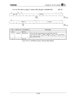
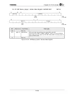
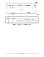
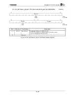
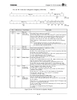
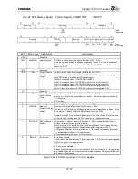
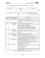
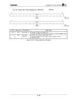
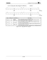
10.4.48 P2G Memory Space 1 Control Register (P2GM1CTR)
0xD18C
31
29
28
20
19
16
Reserved AM[28:20]
Reserved
R/W
: Type
0x03F
:
Initial
value
15 11
10 8 7 5 4 3 2 1 0
Reserved
TPRBL
Reserved
TMCC
Reserved MEM1PE
P2GM1EN
BSWAP
R/W
R/W
R/W
R/W
R/W
R/W
:
Type
010
0
1
1
0
0/1
:
Initial
value
Bits Mnemonic Field
Name
Description
31:29
⎯
Reserved
⎯
28:20
AM[28:20]
Address Mask
PCI-Bus to G-Bus Address Mask (Initial value: 0x03F, R/W)
Sets the bits to be subject to address comparison. See 10.3.4 for more information.
When setting a memory space size of 256 MB (0x1000_0000) for example, the value
becomes 0x0FF.
19:11
⎯
Reserved
⎯
10:8 TPRBL
Target Prefetch
Read Burst
Length
Target Prefetch Read Burst Length (Initial value: 0x3, R/W)
These bits set the G-Bus Burst Size (in DWORDS, (32-bit words)) to be read into the
data FIFO during a target memory Read operation.
0x000: Access and transfer 1DWORD (NO BURST)
0x001: Access and transfer 4 DWORDs of data to the target read FIFO.
0x010: Access and transfer 8 DWORDs of data to the target read FIFO.
0x011: Access and transfer 16 DWORDs of data to the target read FIFO.
0x1xx: Access and transfer 32 DWORDs of data to the target read FIFO.
7:5
⎯
Reserved
⎯
4 TMCC
Target Memory
space 1 Cache
Clear
Target Memory space 1 Cache Clear (Initial value: 0, R/W)
A write of 1 will flush the Target Memory Cache 1. This bit is cleared automatically.
1: Cache Clear
0: Don’t care
3
⎯
Reserved
Note: This bit is always set to “0”. (Initial value: 1, R/W)
2 MEM1PE
Memory 1
Window Prefetch
Enable
Memory 1 Window Prefetch Enable (Initial value: 1, R/W)
If this bit is set, Prefetching of G-Bus data will occur on Target Memory Reads. If this
bit is cleared, 1 Burst of length TPRBL will be done on the G-Bus.
Even if the setting of this bit is changed, prefetchable bits in the Base Address
Register of the PCI Configuration Space will not reflect this change. We recommend
using the default setting when the PCI Controller is in the Satellite mode.
1 P2GM1EN
Memory Space 1
Enable
Target Memory Space 1 Enable (Initial value: 0, R/W) Controls whether Memory
Space 1 for target access is valid or invalid.
When this bit is set to invalid, Writes to the Memory Space 1 Lower Base Address
Register or the Memory Space 1 Upper Base Address Register of the PCI
Configuration Register become invalid. Also, “1” is returned to Reads as a response.
1: Validates Memory Space 1 for target access.
0: Invalidates Memory Space 1 for target access.
0
BSWAP
Byte Swap
Byte Swap Disable
(Initial value: Little Endian Mode: 0; Big Endian Mode: 1, R/W) Sets the byte swapping
of Memory Space 1 for target access.
0: Do not perform byte swapping.
1: Perform byte swapping.
Please use the default state in most situations. If this bit is changed to “0” when in the
Big Endian Mode, the byte order of transfer to Memory Space 0 through DWORD (32-
bit) access will not change.
Figure 10.4.48 P2G Memory Space 1 Control Register
Summary of Contents for TMPR4925
Page 1: ...64 Bit TX System RISC TX49 Family TMPR4925 Rev 3 0 ...
Page 4: ......
Page 15: ...Handling Precautions ...
Page 16: ......
Page 18: ...1 Using Toshiba Semiconductors Safely 1 2 ...
Page 40: ...3 General Safety Precautions and Usage Considerations 3 18 ...
Page 42: ...4 Precautions and Usage Considerations 4 2 ...
Page 43: ...TMPR4925 ...
Page 44: ......
Page 54: ...Chapter 1 Features 1 8 ...
Page 58: ...Chapter 2 Block Diagram 2 4 ...
Page 88: ...Chapter 4 Address Mapping 4 12 ...
Page 226: ...Chapter 8 DMA Controller 8 58 ...
Page 260: ...Chapter 9 SDRAM Controller 9 34 ...
Page 480: ...Chapter 15 Interrupt Controller 15 32 ...
Page 554: ...Chapter 19 Real Time Clock RTC 19 8 ...
Page 555: ...Chapter 20 Removed 20 1 20 Removed ...
Page 556: ...Chapter 20 Removed 20 2 ...
Page 564: ...Chapter 21 Extended EJTAG Interface 21 8 ...
Page 580: ...Chapter 22 Electrical Characteristics 22 16 ...
Page 588: ...Chapter 24 Usage Notes 24 2 ...

