Chapter 10 PCI Controller
10-94
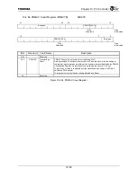
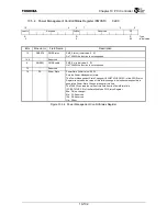
10.4.65 PDMAC Configuration Register (PDMCFG)
0xD210
31
22
21
20
19
18
16
Reserved
RSTFIFO
BSWAP
GBRSTI
Reserved
R/W
R/W
R/W
:
Type
0
0
0
:
Initial
value
15
14
13 11
10 9 8 7 6 5 4 3 2 1 0
Reserved REQDLY
ERRIE
NCCMPIE NTCMPIE
CHNEN
XFRACT
Reserved
XFRMODE
XFRDIRC
CHRST
R/W R/W
R/W
R/W R R/W
R/W R/W
R/W
:
Type
000 0 0 0 0 0
00
0 1
:
Initial
value
Bits Mnemonic Field
Name
Description
31:22
⎯
Reserved
⎯
21
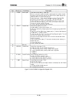
RSTFIFO
Reset FIFO
Reset FIFO (Initial value: 0, R/W)
Initializes the Read pointer and Write pointer to the FIFO in the PDMAC, and sets the
FIFO hold count to “0”. Please use the software to clear this bit when it is set.
1: Performs FIFO reset.
0: Does not perform FIFO reset.
20 BSWAP
Byte Swap Within
DWORD
Swap Bytes in DWORD (Initial value: 0, R/W)
Specifies whether to perform 32-bit data byte swapping.
Please leave this bit at “0” for normal usage.
Setting this bit when in the Big Endian mode executes data transfer so the byte order
of the 32-bit data on the PCI Bus (which is Little Endian) does not change.
1: Transfer without swapping the byte order of each 32-bit DWORD data.
0: Swap the byte order of each 32-bit DWORD data, then transfer.
19 GBRSTI
G-Bus Burst
Inhibit
G-Bus Burst Inhibit (Initial value: 0, R/W)
1: Do not use burst operations on G-Bus even if the burst mode field specifies burst.
This allows devices that can’t burst to transfer data using bursts on the PCI bus.
This bit applies only to G-Bus data transfers; it has no affect on chain operations.
0: The MDA will use burst operations for G-Bus data transfers when programmed to
do so and if alignment, count, etc. permit.
18:14
⎯
Reserved
⎯
13:11 REQDLY
Request Delay
Time
Request Delay (Initial value: 0x0, R/W)
G-Bus transactions for DMA transfer must be performed separated at least by the
interval this field specifies.
000: Continuously try to perform G-Bus transfer.
001: 16 G-Bus clocks
010: 32 G-Bus clocks
011: 64 G-Bus clocks
100: 128
G-Bus clocks
101: 256
G-Bus clocks
110: 512
G-Bus clocks
111: 1024 G-Bus clocks
10 ERRIE
Error Detect
Interrupt Enable
Interrupt Enable on Error (Initial value: 0, R/W)
1: PDMAC generates an error during error detection.
0: PDMAC does not generate an error during error detection.
9 NCCMPIE
Normal Chain
Complete
Interrupt Enable
Interrupt Enable on Chain Done (Initial value: 0, R/W)
1: PDMAC generates an interrupt when the current chain is complete.
0: PDMAC does not generate an interrupt when the current chain is complete.
8 NTCMPIE
Normal Data
Transfer
Complete
Interrupt Enable
Interrupt Enable on Transfer Done (Initial value: 0, R/W)
1: PDMAC generates an interrupt when the current data transfer is complete.
0: PDMAC does not generate an interrupt when the current data transfer is complete.
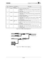
Figure 10.4.65 PDMAC Configuration Register (1/2)
Summary of Contents for TMPR4925
Page 1: ...64 Bit TX System RISC TX49 Family TMPR4925 Rev 3 0 ...
Page 4: ......
Page 15: ...Handling Precautions ...
Page 16: ......
Page 18: ...1 Using Toshiba Semiconductors Safely 1 2 ...
Page 40: ...3 General Safety Precautions and Usage Considerations 3 18 ...
Page 42: ...4 Precautions and Usage Considerations 4 2 ...
Page 43: ...TMPR4925 ...
Page 44: ......
Page 54: ...Chapter 1 Features 1 8 ...
Page 58: ...Chapter 2 Block Diagram 2 4 ...
Page 88: ...Chapter 4 Address Mapping 4 12 ...
Page 226: ...Chapter 8 DMA Controller 8 58 ...
Page 260: ...Chapter 9 SDRAM Controller 9 34 ...
Page 480: ...Chapter 15 Interrupt Controller 15 32 ...
Page 554: ...Chapter 19 Real Time Clock RTC 19 8 ...
Page 555: ...Chapter 20 Removed 20 1 20 Removed ...
Page 556: ...Chapter 20 Removed 20 2 ...
Page 564: ...Chapter 21 Extended EJTAG Interface 21 8 ...
Page 580: ...Chapter 22 Electrical Characteristics 22 16 ...
Page 588: ...Chapter 24 Usage Notes 24 2 ...


