Chapter 14 AC-link Controller
14-19
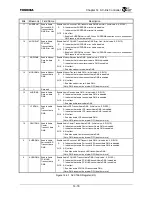
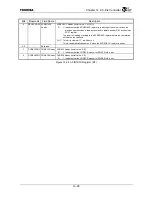
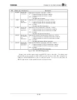
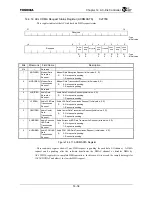
Bits Mnemonic Field
Name
Description
7:6
⎯
Reserved
⎯
Clear CODEC Ready Bit (Initial value: 0, W1S)
W1C 0: No effect
1: Clear CODEC[1:0] ready bits
5 RDYCLR
Clear CODEC
Ready Bit
Note: This bit should only be written to reevaluate the CODEC ready status after power-
down command is sent to CODEC.
MIC Selection. (Initial value: 0, R/W1S)
4
MICSEL MIC
Selection
R
0: Indicates that PCM L&R (Slot 3&4) is selected for audio reception.
1: Indicates that MIC (Slot 6) is selected for audio reception.
W1S 0: No effect
1: Selects MIC (Slot 6) for audio reception.
Assert Warm Reset. (Initial value: 0, R/W1S)
3
WRESET
Assert Warm
Reset
R
0: Indicates that warm reset is not asserted.
1: Indicates that warm reset is asserted.
W1S 0: No effect
1: Asserts warm reset.
Note 1: Do not assert warm reset during normal operation.
Note 2: The software must guarantee the warm reset assertion time meets the AC’97
specification (1.0
µ
s or more).
Enable Wake-up. (Initial value: 0, R/W1S)
2
WAKEUP Enable
Wake-up
R
0: Indicates that wake-up from low-power mode is disabled.
1: Indicates that wake-up from low-power mode is enabled. While any SDIN signal
is driven high, ACLC asserts ACLCPME interrupt request to the interrupt
controller.
W1S 0: No effect
1: Enables wake-up from low-power mode.
Note: Do not enable wake-up during normal operation.
Enable AC-link Low-power Mode. (Initial value: 0, R/W1S)
1
LOWPWR
Enable AC-link
low-power mode
R
0: SYNC and SDOUT signals are not forced to low.
1: SYNC and SDOUT signals are forced to low.
W1S 0: No effect
1: Forces SYNC and SDOUT signals low.
Note: Do not enable AC-link low-power mode during normal operation.
Enable AC-link. (Initial value: 0, R/W1S)
0
ENLINK Enable
AC-link
R
0: Indicates that the ACRESET
*
signal to AC-link is asserted.
1: Indicates that the ACRESET
*
signal to AC-link is not asserted.
W1S 0: No effect
1: Deasserts the ACRESET
*
signal to AC-link
Note: The software must guarantee the ACRESET
*
signal assertion time meets the AC’97
specification (1.0
µ
s or more).
Figure 14.4.1 ACCTLEN Register (3/3)
Summary of Contents for TMPR4925
Page 1: ...64 Bit TX System RISC TX49 Family TMPR4925 Rev 3 0 ...
Page 4: ......
Page 15: ...Handling Precautions ...
Page 16: ......
Page 18: ...1 Using Toshiba Semiconductors Safely 1 2 ...
Page 40: ...3 General Safety Precautions and Usage Considerations 3 18 ...
Page 42: ...4 Precautions and Usage Considerations 4 2 ...
Page 43: ...TMPR4925 ...
Page 44: ......
Page 54: ...Chapter 1 Features 1 8 ...
Page 58: ...Chapter 2 Block Diagram 2 4 ...
Page 88: ...Chapter 4 Address Mapping 4 12 ...
Page 226: ...Chapter 8 DMA Controller 8 58 ...
Page 260: ...Chapter 9 SDRAM Controller 9 34 ...
Page 480: ...Chapter 15 Interrupt Controller 15 32 ...
Page 554: ...Chapter 19 Real Time Clock RTC 19 8 ...
Page 555: ...Chapter 20 Removed 20 1 20 Removed ...
Page 556: ...Chapter 20 Removed 20 2 ...
Page 564: ...Chapter 21 Extended EJTAG Interface 21 8 ...
Page 580: ...Chapter 22 Electrical Characteristics 22 16 ...
Page 588: ...Chapter 24 Usage Notes 24 2 ...


