Chapter 14 AC-link Controller
14-21
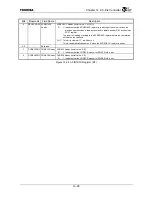
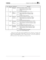
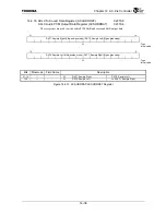
Bits Mnemonic Field
Name
Description
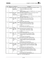
13
⎯
Reserved
⎯
Disable Audio Receive-data DMA. (Initial value: –, W1C)
12 AUDIDMA
Disable Audio
Receive-data
DMA
W1C 0: No effect
1: Disables audio receive-data DMA.
Disable Audio LFE Transmit-data DMA. (Initial value: –, W1C)
11 LFEDMA
Disable Audio
LFE Transmit-
data DMA
W1C 0: No effect
1: Disables audio LFE transmit-data DMA.
Disable Audio Center Transmit-data DMA. (Initial value: –, W1C)
10 CENTDMA
Disable Audio
Center
Transmit-data
DMA
W1C 0: No effect
1: Disables audio Center transmit-data DMA.
Disable Audio Surround L&R Transmit-data DMA. (Initial value: –, W1C)
9 SURRDMA
Disable Audio
Surround L&R
Transmit-data
DMA
W1C 0: No effect
1: Disables audio Surround L&R transmit-data DMA.
Disable Audio PCM L&R Transmit-data DMA. (Initial value: –, W1C)
8 AUDODMA
Disable Audio
PCM L&R
Transmit-data
DMA
W1C 0: No effect
1: Disables audio PCM L&R transmit-data DMA.
7:5
⎯
Reserved
⎯
MIC Selection (Initial value: –, W1C)
4 MICSEL
MIC
Selection
W1C 0: No effect
1: Selects PCM L&R (Slot 3&4) for audio reception
Deassert Warm Reset. (Initial value: –, W1C)
W1C 0: No effect
1: Deasserts warm reset.
3 WRESET
Deassert Warm
Reset
Note: The software must guarantee the warm reset assertion time meets the AC’97
specification (1.0
µ
s or more).
Disable Wake-up. (Initial value: –, W1C)
2 WAKEUP
Disable Wake-
up.
W1C 0: No effect
1: Disables wake-up from low-power mode.
Disable AC-link Low-power Mode. (Initial value: –, W1C)
1 LOWPWR
Disable AC-link
Low-power
Mode.
W1C 0: No effect
1: Releases SYNC and SDOUT signals from low.
Disable AC-link. (Initial value: –, W1C)
W1C 0: No effect
1: Asserts the ACRESET
*
signal to AC-link.
0 ENLINK
Disable
AC-link
Note: The software must guarantee the ACRESET
*
signal assertion time meets the AC’97
specification (1.0
µ
s or more).
Figure 14.4.2 ACCTLDIS Register (2/2)
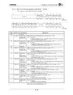
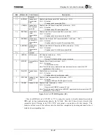
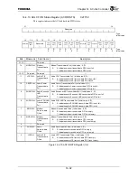
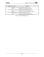
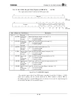
Clear xxxxDMA bits in ACCTLEN to “0” by using this register to disable transmit/receive-data
DMA and to stop transmission/reception by the AC-link. Note that if these bits are cleared while
output-slot data is flowing in the FIFO, ACLC may output a wrong data as the last sample. This
behavior will not occur if the software waits for data-flow completion by detecting underrun before it
disables the corresponding slot.
Summary of Contents for TMPR4925
Page 1: ...64 Bit TX System RISC TX49 Family TMPR4925 Rev 3 0 ...
Page 4: ......
Page 15: ...Handling Precautions ...
Page 16: ......
Page 18: ...1 Using Toshiba Semiconductors Safely 1 2 ...
Page 40: ...3 General Safety Precautions and Usage Considerations 3 18 ...
Page 42: ...4 Precautions and Usage Considerations 4 2 ...
Page 43: ...TMPR4925 ...
Page 44: ......
Page 54: ...Chapter 1 Features 1 8 ...
Page 58: ...Chapter 2 Block Diagram 2 4 ...
Page 88: ...Chapter 4 Address Mapping 4 12 ...
Page 226: ...Chapter 8 DMA Controller 8 58 ...
Page 260: ...Chapter 9 SDRAM Controller 9 34 ...
Page 480: ...Chapter 15 Interrupt Controller 15 32 ...
Page 554: ...Chapter 19 Real Time Clock RTC 19 8 ...
Page 555: ...Chapter 20 Removed 20 1 20 Removed ...
Page 556: ...Chapter 20 Removed 20 2 ...
Page 564: ...Chapter 21 Extended EJTAG Interface 21 8 ...
Page 580: ...Chapter 22 Electrical Characteristics 22 16 ...
Page 588: ...Chapter 24 Usage Notes 24 2 ...


