Chapter 16 CHI Module
16-7
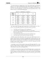
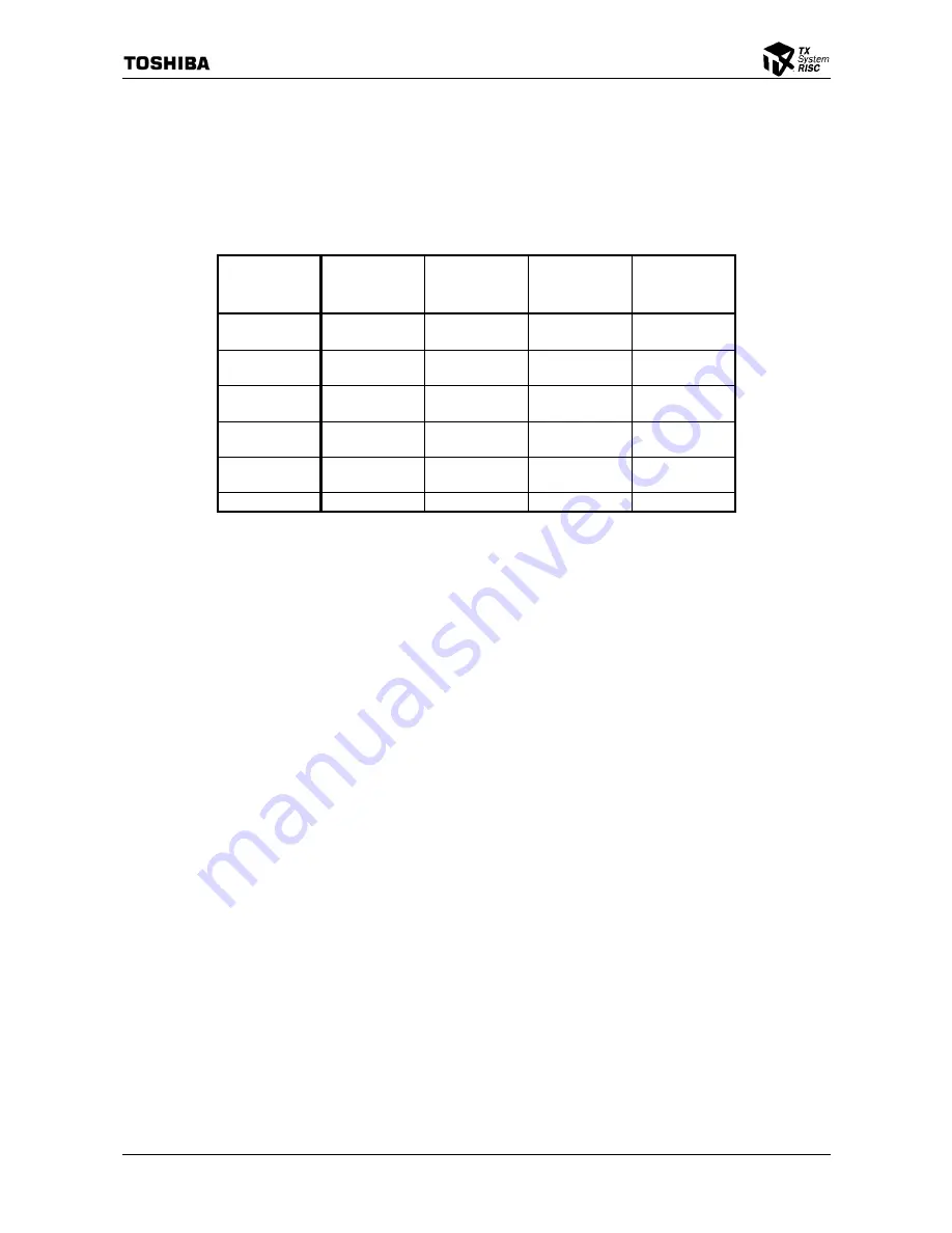
Note that the byte lanes are swapped between the little- and big-endian modes. In the little-endian
mode, bits 31:24 of a word on the DMA buffer correspond to the byte lane with the address offset ‘+3’
and therefore to the ‘byte0’ in the CHI TX/RX holding register. On the contrary, in the big-endian mode,
bits 31:24 of a word on the DMA buffer correspond to the byte lane with the address offset ‘+0’ and
therefore to the ‘byte3’ in the CHI TX/RX holding register.
Table 16.3.1 CHI DMA Memory Organization
(Relative)
Memory
Address
+0 +1 +2 +3
+0x0
buffA, byte3
buffA, byte2
buffA, byte1
buffA, byte0
sample 0
sample 0
sample 0
sample 0
+0x4
buffB, byte3
buffB, byte2
buffB, byte1
buffB, byte0
sample 0
sample 0
sample 0
sample 0
+0x8
buffA, byte3
buffA, byte2
buffA, byte1
buffA, byte0
sample 1
sample 1
sample 1
sample 1
+0xC
buffB, byte3
buffB, byte2
buffB, byte1
buffB, byte0
sample 1
sample 1
sample 1
sample 1
+0x10
buffA, byte3
buffA, byte2
buffA, byte1
buffA, byte0
sample 2
sample 2
sample 2
sample 2
etc.
For a given channel, the minimum input-to-output latency for the CHI data path is (4 cycles)
×
(62.5
µ
s) = 250
µ
s, assuming an 8 kHz frame rate. These required 4 cycles are as follows:
•
1 cycle to load receive shift register into receive holding register
•
1 cycle for DMA of receive holding register data into receive memory space
(insert here any application-specific time required for processing of received data and moving
result to transmit memory space)
•
1 cycle for DMA of data in transmit memory space to transmit holding register
•
1 cycle to load transmit holding register data into transmit shift register
Half-buffer and end-of-buffer DMA address counter interrupts are available, allowing the CPU to
minimize overhead and utilize the DMA buffer in a ping-pong fashion. For transmit mode, the CPU can
use these interrupts to fill or write one half of the buffer while the other half is being emptied by the
DMA controller for transmitting out the CHI. Similarly, for receive mode, the CPU can use these
interrupts to empty or read one half of the buffer while the other half is being filled by the DMA
controller from received CHI input samples.
Also available is a direct CPU read/write mode for bypassing the DMA, allowing the CPU to read or
write the CHI data on a sample by sample basis, if so desired. Separate DMA enables for receive and
transmit allow DMA to be setup for receive only (transmit via CPU), transmit only (receive via CPU),
receive and transmit, or none (receive and transmit via CPU).
The DMA circuit also provides an interrupt each time the DMA buffer pointer is incremented, which
occurs whenever a new sample is read from and/or written to the DMA buffer. This interrupt may be
useful for triggering a read of the DMA pointer status value, which is the actual 12-bit DMA address
counter output. This value indicates exactly where the current address is pointing to in the overall DMA
buffer.
Summary of Contents for TMPR4925
Page 1: ...64 Bit TX System RISC TX49 Family TMPR4925 Rev 3 0 ...
Page 4: ......
Page 15: ...Handling Precautions ...
Page 16: ......
Page 18: ...1 Using Toshiba Semiconductors Safely 1 2 ...
Page 40: ...3 General Safety Precautions and Usage Considerations 3 18 ...
Page 42: ...4 Precautions and Usage Considerations 4 2 ...
Page 43: ...TMPR4925 ...
Page 44: ......
Page 54: ...Chapter 1 Features 1 8 ...
Page 58: ...Chapter 2 Block Diagram 2 4 ...
Page 88: ...Chapter 4 Address Mapping 4 12 ...
Page 226: ...Chapter 8 DMA Controller 8 58 ...
Page 260: ...Chapter 9 SDRAM Controller 9 34 ...
Page 480: ...Chapter 15 Interrupt Controller 15 32 ...
Page 554: ...Chapter 19 Real Time Clock RTC 19 8 ...
Page 555: ...Chapter 20 Removed 20 1 20 Removed ...
Page 556: ...Chapter 20 Removed 20 2 ...
Page 564: ...Chapter 21 Extended EJTAG Interface 21 8 ...
Page 580: ...Chapter 22 Electrical Characteristics 22 16 ...
Page 588: ...Chapter 24 Usage Notes 24 2 ...


