Chapter 17 Serial Peripheral Interface
17-3
17.3 Detailed
Explanation
17.3.1 Operation
mode
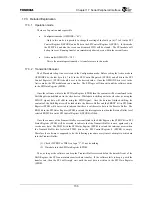
There are 2 operation modes possible:
•
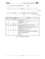
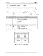
Configuration mode (OPMODE = ‘01’) :
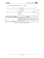
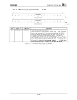
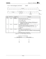
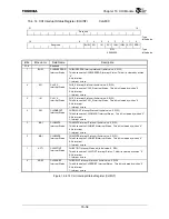
Only in this mode it is possible to change the setting of the low byte (bit 7 to 0) in the SPI
Control Register 0 (SPCR0) and all bits in the SPI Control Register 1 (SPCR1). In this mode
the SPSTP bit and also the receive and transmit FIFO will be cleared. The SPI module will
be kept in reset. Running transfer are immediately aborted, even within the current frame.
•
Active mode (OPMODE = ‘10’) :
This is the normal operation mode. A transfer occurs in this mode.
17.3.2 Transmitter/Receiver
The SPI module is kept in a reset state in the Configuration mode. Before setting the Active mode in
OPMODE bits, the low byte (bit 7 to 0) in the SPI Control Register 0 (SPCR0) and all bits in the SPI
Control Register 1 (SPCR1) should be set to the desired value. Once the OPMODE bits is set to the
Active mode, the SPI module can run a transfer. The SPI logic will then wait until the software writes
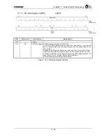
to the SPI Data Register (SPDR).
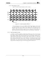
Once the software writes to the SPI Data Register (SPDR) then the contents will be transferred to the
Shift Register and shifted out to the slave device. While data is shifting out to the slave device using the
SPIOUT signal, data will shift in using the SPIIN signal. Once the data has finished shifting, the
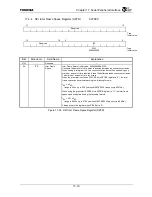
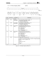
contents of the Shift Register will be loaded into the Receive Buffer and the SRRDY bit in SPI Status
Register (SPSR) will be asserted to indicate that there is valid receive data in the Receive Buffer. The
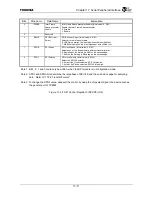
RBSI bit in the SPI Status Register (SPSR) is set and the interrupt occurs when the Receive Buffer level
selected RXIFL bits in the SPI Control Register 0 (SPCR0) is filled.
Once the contents of the Transmit Buffer are transferred to the Shift Register, the STRDY bit in SPI
Status Register (SPSR) will be asserted to indicate that the Transmit Buffer is once again ready to
receive new data. The TBSI bit in the SPI Status Register (SPSR) is set and the interrupt occurs when
the Transmit Buffer level selected TXIFL bits in the SPI Control Register 0 (SPCR0) is empty.
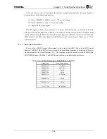
Therefore the software is supposed to do the following procedure every time it attempts to write data
into the Transmit Buffer.
(1) Check if STRDY or TBSI is a logic “1”. If not, do nothing.
(2) Write data into the SPI Data Register (SPDR).
Thus, as long as the software can keep the Transmit Buffer serviced before the data shifts out of the
Shift Register, the SPI can maintain seamless data transfer. If the software fails to keep up with the
transfer rate, then the SPI will simply wait until the next data is written to the SPI Data Register
(SPDR).
Summary of Contents for TMPR4925
Page 1: ...64 Bit TX System RISC TX49 Family TMPR4925 Rev 3 0 ...
Page 4: ......
Page 15: ...Handling Precautions ...
Page 16: ......
Page 18: ...1 Using Toshiba Semiconductors Safely 1 2 ...
Page 40: ...3 General Safety Precautions and Usage Considerations 3 18 ...
Page 42: ...4 Precautions and Usage Considerations 4 2 ...
Page 43: ...TMPR4925 ...
Page 44: ......
Page 54: ...Chapter 1 Features 1 8 ...
Page 58: ...Chapter 2 Block Diagram 2 4 ...
Page 88: ...Chapter 4 Address Mapping 4 12 ...
Page 226: ...Chapter 8 DMA Controller 8 58 ...
Page 260: ...Chapter 9 SDRAM Controller 9 34 ...
Page 480: ...Chapter 15 Interrupt Controller 15 32 ...
Page 554: ...Chapter 19 Real Time Clock RTC 19 8 ...
Page 555: ...Chapter 20 Removed 20 1 20 Removed ...
Page 556: ...Chapter 20 Removed 20 2 ...
Page 564: ...Chapter 21 Extended EJTAG Interface 21 8 ...
Page 580: ...Chapter 22 Electrical Characteristics 22 16 ...
Page 588: ...Chapter 24 Usage Notes 24 2 ...


