Chapter 18 NAND Flash Memory Controller
18-2
18.3 Detailed
Explanation
18.3.1 Access to NAND Flash Memory
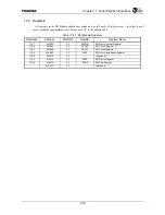
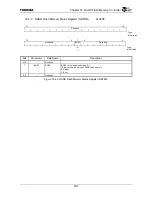
The TX4925 NDFMC supports the interface between the NAND Flash Memory using register
indirect sequence. It has the ECC calculating circuits. Please see 18.3.2 in detail of the ECC. This
section describes the procedure to access to NAND Flash Memory.
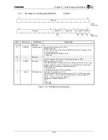
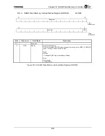
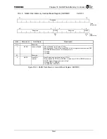
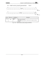
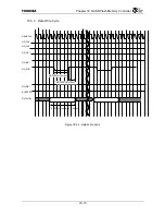
Basically, set the command in NDFMCR at first and then read or write in NDFDTR. The read cycle
for NDFDTR is finished after the external read cycle for the NAND Flash Memory is finished. Equally,
the write cycle for NDFDTR is finished after the external write cycle for the NAND Flash Memory is
finished.
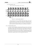
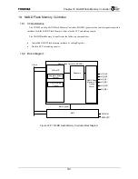
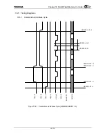
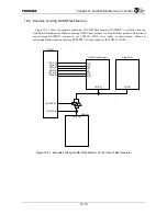
To connect external NAND flash memory using bus separate (refer to Figure 18.6.1), set
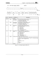
NDFMCR.BSPRT (Bus Separate bit) and assert the BUSSPRT* signal.
18.3.1.1 Initialize
The initialize sequence is below.
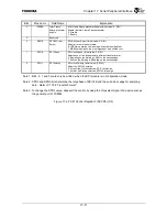
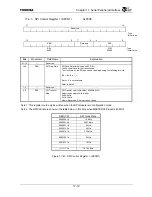
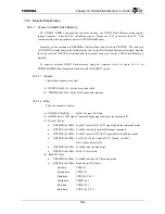
(1) NDFSPR (0xC014): Set the Low pulse width.
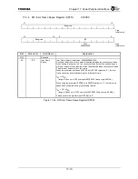
(2) NDFIMR (0xC010): Set 0x81 if need enable interrupt.
18.3.1.2 Write
The write sequence is below.
(1) NDFMCR (0xC004):
Set 0x70 to reset ECC data.
(2) NDFMC hasn’t WP* signal. It must be high using other logic for example PIO.
(3) Write
512
bytes
•
NDFMCR (0xC004): Set 0x91 to assert ND_CLE* signal and do the command mode.
•
NDFDTR (0xC000): Set 0x80 to write the Serial Data Input command.
•
NDFMCR (0xC004): Set 0x92 to assert ND_ALE* signal and do the address mode.
•
NDFDTR (0xC000): Set A[7:0], A[16:9], and A[24:17]. If need, set A[25].
Note: It does not set A[8].
•
NDFMCR (0xC004): Set 0xb0 to do the data mode.
•
NDFDTR (0xC000): Write 512 bytes data.
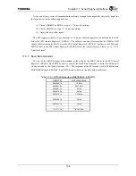
(4) Read ECC data
•
NDFMCR (0xC004): Set 0xd0 to do the ECC data read mode.
•
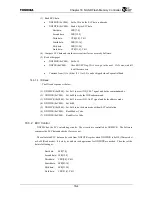
NDFDTR (0xC000): Read 6 bytes ECC data.
First
data:
LPR[7:0]
Second
data: LPR[15:8]
Third data:
CPR[5:0], 2’b11
Fourth
data: LPR[23:16]
Fifth
data:
LPR[31:24]
Sixth data:
CPR[11:6], 2’b11
Summary of Contents for TMPR4925
Page 1: ...64 Bit TX System RISC TX49 Family TMPR4925 Rev 3 0 ...
Page 4: ......
Page 15: ...Handling Precautions ...
Page 16: ......
Page 18: ...1 Using Toshiba Semiconductors Safely 1 2 ...
Page 40: ...3 General Safety Precautions and Usage Considerations 3 18 ...
Page 42: ...4 Precautions and Usage Considerations 4 2 ...
Page 43: ...TMPR4925 ...
Page 44: ......
Page 54: ...Chapter 1 Features 1 8 ...
Page 58: ...Chapter 2 Block Diagram 2 4 ...
Page 88: ...Chapter 4 Address Mapping 4 12 ...
Page 226: ...Chapter 8 DMA Controller 8 58 ...
Page 260: ...Chapter 9 SDRAM Controller 9 34 ...
Page 480: ...Chapter 15 Interrupt Controller 15 32 ...
Page 554: ...Chapter 19 Real Time Clock RTC 19 8 ...
Page 555: ...Chapter 20 Removed 20 1 20 Removed ...
Page 556: ...Chapter 20 Removed 20 2 ...
Page 564: ...Chapter 21 Extended EJTAG Interface 21 8 ...
Page 580: ...Chapter 22 Electrical Characteristics 22 16 ...
Page 588: ...Chapter 24 Usage Notes 24 2 ...

