Chapter 3 Signals
3-4
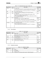
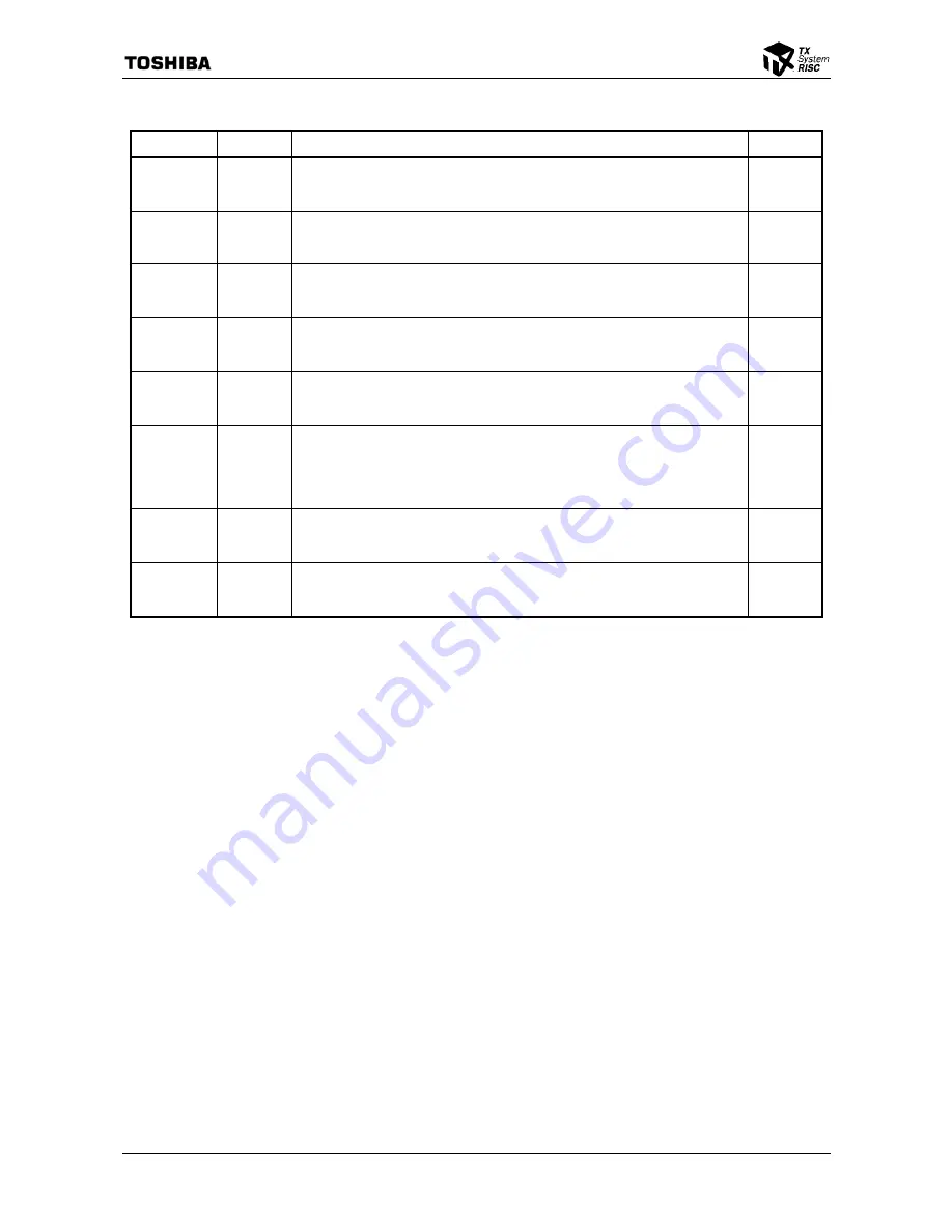
Table 3.1.3 External Interface Signals (2/2)
Signal Name
Type
Description
Initial State
CARD1CSH
*
CARD1CSL
*
Output
PU
PCMCIA card slot 1 chip select
Chip select signals for PCMCIA card slot 1.
The pins are shared with other functions (refer to Section "3.3 Pin Multiplexing").
PIO input
CARD2CSH
*
CARD2CSL
*
Output
PU
PCMCIA card slot 2 chip select
Chip select signals for PCMCIA card slot 2.
The pins are shared with other functions (refer to Section "3.3 Pin Multiplexing").
PIO input
CARDREG
*
Output
PU
PCMCIA card register
REG
*
signal for a PCMCIA card.
The pin is shared with other functions (refer to Section "3.3 Pin Multiplexing").
PIO input
CARDIORD
*
Output
PU
PCMCIA card I/O read
IORD
*
signal for a PCMCIA card.
The pin is shared with other functions (refer to Section "3.3 Pin Multiplexing").
PIO input
CARDIOWR
*
Output
PU
PCMCIA card I/O write
IOWR
*
signal for a PCMCIA card.
The pin is shared with other functions (refer to Section "3.3 Pin Multiplexing").
PIO input
CARDDIR
*
Output
PU
PCMCIA card directory
Controls the direction of the bidirectional buffer used for a PCMCIA slot. This signal is
asserted during a read transaction when any of CARD2CSH
*
, CARD2CSL
*
,
CARD1CSH
*
and CARD1CSL
*
are asserted.
The pin is shared with other functions (refer to Section "3.3 Pin Multiplexing").
PIO input
CARD1WAIT
*
Input
PU
PCMCIA card slot 1 wait
Card wait signal from PCMCIA card slot 1.
The pin is shared with other functions (refer to Section "3.3 Pin Multiplexing").
PIO input
CARD2WAIT
*
Input
PU
PCMCIA card slot 2 wait
Card wait signal from PCMCIA card slot 2.
The pin is shared with other functions (refer to Section "3.3 Pin Multiplexing").
PIO input
Summary of Contents for TMPR4925
Page 1: ...64 Bit TX System RISC TX49 Family TMPR4925 Rev 3 0 ...
Page 4: ......
Page 15: ...Handling Precautions ...
Page 16: ......
Page 18: ...1 Using Toshiba Semiconductors Safely 1 2 ...
Page 40: ...3 General Safety Precautions and Usage Considerations 3 18 ...
Page 42: ...4 Precautions and Usage Considerations 4 2 ...
Page 43: ...TMPR4925 ...
Page 44: ......
Page 54: ...Chapter 1 Features 1 8 ...
Page 58: ...Chapter 2 Block Diagram 2 4 ...
Page 88: ...Chapter 4 Address Mapping 4 12 ...
Page 226: ...Chapter 8 DMA Controller 8 58 ...
Page 260: ...Chapter 9 SDRAM Controller 9 34 ...
Page 480: ...Chapter 15 Interrupt Controller 15 32 ...
Page 554: ...Chapter 19 Real Time Clock RTC 19 8 ...
Page 555: ...Chapter 20 Removed 20 1 20 Removed ...
Page 556: ...Chapter 20 Removed 20 2 ...
Page 564: ...Chapter 21 Extended EJTAG Interface 21 8 ...
Page 580: ...Chapter 22 Electrical Characteristics 22 16 ...
Page 588: ...Chapter 24 Usage Notes 24 2 ...

