Chapter 8 DMA Controller
8-13
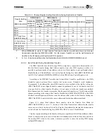
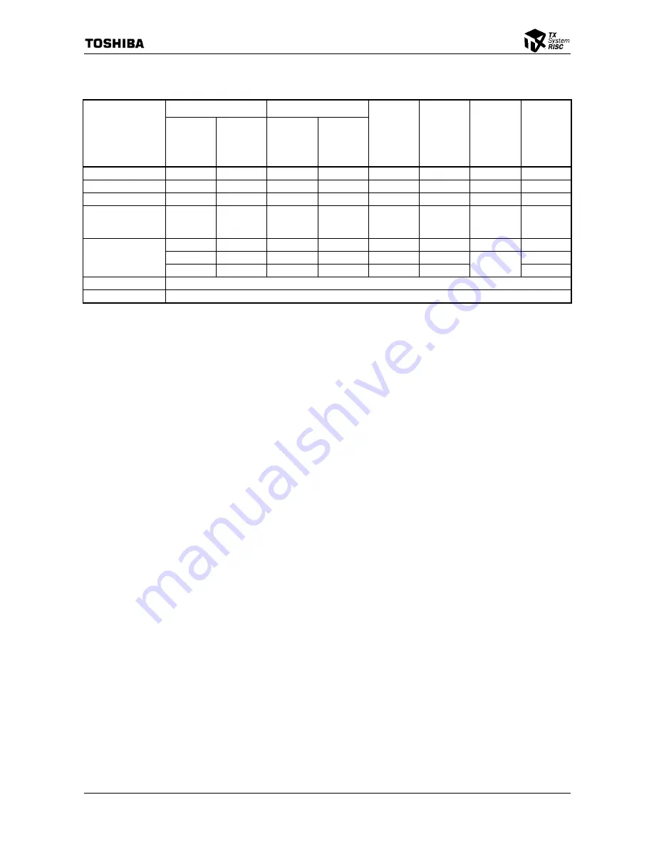
Table 8.3.3 Channel Register Setting Restrictions During Dual Address Transfer
DMSARn[2:0] DMDARn[2:0]
Transfer Setting
Size
(DMCCRn.XFSZ)
DMSAIRn
setting is 0
or greater
DMSAIRn
setting is a
negative
value
DMDAIRn
setting is 0
or greater
DMDAIRn
setting is a
negative
value
DMSAIRn DMDAIRn DMCNTRn
DMCCRn
REVBYTE
1 Byte
*** *** *** *** *** *** ***
0
2 Bytes
**
0
**
0
**
0
**
1
**
0
**
0
**
0 0
4 Bytes
*
00
*
00
*
00
*
11
*
00
*
00
*
00 0
8 Bytes,
4 / 8 Double Wods
(DMMCR.FIFUM[n]
=
0)
000 111 000 111 000 000 000 0/1
000 111 000 111
8/0/-8
g
8/-8
‡ 000
0/1
***
⎯
***
⎯
8 8
0
4 / 8 Double Words
(DMMCR.FIFUM[n]
=
1)
⎯
***
⎯
***
-8 -8
***
0
16 Double Words
Cannot be set (Configuration Error)
32 Double Words
Cannot be set (Configuration Error)
g
:
When DMSAIRn is set to 0, read access from source device is performed only one time per
transmission specified by DMCCRn.XFSZ. For this reason, transfer can not be performed burst
transfer to the I/O device which performs FIFO operation.
‡:
8, 0, or -8 can be specified when the Destination Burst Inhibit bit (DMCCRn.DBINH) is set.
8.3.8.2 Burst Transfer During Dual Address Transfer
The DMA Controller has a 64-bit 8-stage FIFO on-chip that is connected to the internal bus (G-
Bus) for Burst transfer during Dual Address transfer. Since this FIFO employs a shifter, it is
possible to perform transfer of any address or data size. Burst transfer is only performed when 4
Double Words or 8 Double Words is set by the Transfer Setting Size field (DMCCRn.XFSZ) and
the FIFO Use Enable bit (DMMCRn.FIFUM[n]) of the DMA Master Control Register is set.
According to the SDRAM Controller and External Bus Controller specifications, the DMA
Controller cannot perform Burst transfer that spans across 32-double word boundaries.
Consequently, if the address that starts DMA transfer is not a multiple of the transfer setting size
(DMCCRn.XFSZ) (is not aligned), transfer cannot be performed by any of the transfer sizes that
were specified by a Burst transfer. Therefore, it is necessary to divide the transfer into multiple
Burst transactions of a transfer size smaller than the specified transfer size. This division method
changes according to the seting of the Transfer Size Mode bit (DMCCRn.USEXFSZ) of the DMA
Channel Control Register and whether or not the address offset relative to the Transfer Setting size
(DMCCRn.XFSZ) is equivalent to the source address and destination address combined.
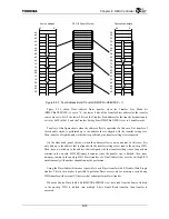
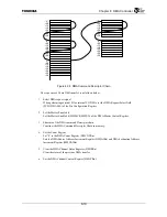
Figure 8.3.3 shows Dual Address Burst transfer when the Transfer Size Mode bit
(DMCCRn.USEXFSZ) is set to “1”, the lower 8 bits of the Transfer Start address for the transfer
source are set to 0xA8, the lower 8 bits of the Transfer Start address for the transfer destination are
set to 0x38, and the Transfer Setting Size (DMCCRn.XFSZ) is set to 8 Double Words.
Transfer repeats according to the transfer setting size, regardless of the different address offsets.
However, transfers that span across 32-double word boundaries are divided. Since data remains in
the on-chip FIFO when in this mode, it becomes possible to share the on-chip FIFO among
multiple DMA channels.
Summary of Contents for TX49 TMPR4937
Page 1: ...64 Bit TX System RISC TX49 Family TMPR4937 Rev 2 0 ...
Page 4: ......
Page 13: ...Table of Contents ix TMPR4937 Revision History 1 ...
Page 14: ...Table of Contents x ...
Page 15: ...Handling Precautions ...
Page 16: ......
Page 18: ...1 Using Toshiba Semiconductors Safely 1 2 ...
Page 40: ...3 General Safety Precautions and Usage Considerations 3 18 ...
Page 42: ...4 Precautions and Usage Considerations 4 2 ...
Page 43: ...TMPR4937 2005 3 Rev 2 0 ...
Page 44: ......
Page 52: ...Chapter 1 Overview and Features 1 6 ...
Page 156: ...Chapter 7 External Bus Controller 7 56 ...
Page 491: ...Chapter 16 Removed 16 1 16 Removed ...
Page 492: ...Chapter 16 Removed 16 2 ...
Page 493: ...Chapter 17 Removed 17 1 17 Removed ...
Page 494: ...Chapter 17 Removed 17 2 ...
Page 495: ...Chapter 18 Removed 18 1 18 Removed ...
Page 496: ...Chapter 18 Removed 18 2 ...
Page 497: ...Chapter 19 Removed 19 1 19 Removed ...
Page 498: ...Chapter 19 Removed 19 2 ...
Page 506: ...Chapter 20 Extended EJTAG Interface 20 8 ...
Page 530: ...Chapter 22 Pinout and Package Information 22 10 ...
Page 542: ...Chapter 24 Parts Number when Ordering 24 2 ...


