Chapter 10 PCI Controller
10-7
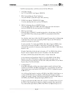
The Memory Read command is issued if these conditions are not met, namely, if “0” is set to
the Cache Line Size field (PCICFG1.CLS) of the PCI Configuration 1 Register. In the case of the
target, a normal G-Bus cycle is issued to the address mapped from the PCI Bus to the G-Bus.
•
Memory Write and Invalidate
When the TX4937 operates as the initiator, the PCI Controller is sue the Memory Write and
Invalidate command if all of the folllowing conditions are met when write access from the G-Bus
to the PCI Bus occurs.
(1) The Memory Write and Invalidate Enable bit (PCISTATUS.MWIEN) of the PCI Status
Command Register is set.
(2) A value other than “0” was set to the Cache Line Size field (PCICFG1.CLS) of the PCI
Configuration 1 Register.
(3) The word count of the Write data is equal to or larger than the value set in the Cache Line
Size field.
The Memory Write command is issued in these conditions are not met.
When the TX4937 operates as the target, the Memory Write and Invalidate command is
converted into G-Bus Write access. Note that the TX4937 does nto support the cache memory
Snoop function.
•
Dual address cycle
When the TX4937 operates as the initiator, the PCI Controller executes dual access cycles if the
PCI Bus address exceeds 0x00_FFFF_FFFF.
When the TX4937 operates as the target, normal G-Bus cycles are executed to the address
mapped from the PCI Bus to the G-Bus.
•
Configuration Read, Configuration Write
These commands only issue configuration cycles as the when in the Host mode.
The corresponding configuration cycles are issued on the PCI Bus. This is done by either
reading or writing from/to the G2P Configuration Data Register (G2PCFGDATA) after writing the
configuration space address to the G2P Configuration Address Register. The TX4937 supports both
“Type 0” and “Type 1” configuration transactions.
On systems that have PCI card slots, the PCI Host device checks each PCI card slot during
system initialization to see if PCI device exist, then set the Configuration Space Register of the
devices that do exist. If a PCI Configuration Read operation is performed for devices that do not
exist, then by default a Bus Error exception will be generated since there is no PCI Bus response.
Clearing the Bus Error Response During Initiator Read bit (PCICFG.IRBER) of the PCI Controller
Configuration Register makes it possible to execute a Read transaction without causing a Bus
Error. All bits of the data read at this time will be set to “1”.
Summary of Contents for TX49 TMPR4937
Page 1: ...64 Bit TX System RISC TX49 Family TMPR4937 Rev 2 0 ...
Page 4: ......
Page 13: ...Table of Contents ix TMPR4937 Revision History 1 ...
Page 14: ...Table of Contents x ...
Page 15: ...Handling Precautions ...
Page 16: ......
Page 18: ...1 Using Toshiba Semiconductors Safely 1 2 ...
Page 40: ...3 General Safety Precautions and Usage Considerations 3 18 ...
Page 42: ...4 Precautions and Usage Considerations 4 2 ...
Page 43: ...TMPR4937 2005 3 Rev 2 0 ...
Page 44: ......
Page 52: ...Chapter 1 Overview and Features 1 6 ...
Page 156: ...Chapter 7 External Bus Controller 7 56 ...
Page 491: ...Chapter 16 Removed 16 1 16 Removed ...
Page 492: ...Chapter 16 Removed 16 2 ...
Page 493: ...Chapter 17 Removed 17 1 17 Removed ...
Page 494: ...Chapter 17 Removed 17 2 ...
Page 495: ...Chapter 18 Removed 18 1 18 Removed ...
Page 496: ...Chapter 18 Removed 18 2 ...
Page 497: ...Chapter 19 Removed 19 1 19 Removed ...
Page 498: ...Chapter 19 Removed 19 2 ...
Page 506: ...Chapter 20 Extended EJTAG Interface 20 8 ...
Page 530: ...Chapter 22 Pinout and Package Information 22 10 ...
Page 542: ...Chapter 24 Parts Number when Ordering 24 2 ...

