Chapter 3 Signals
3-4
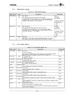
3.1.4
DMA Interface Signals
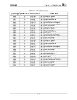
Table 3.1.4 DMA Interface Signals
Signal Name
Type
Description
Initial State
DMAREQ[3:0] Input
PU
DMA Request
DMA transfer request signals from an external I/O device.
The DMAREQ[2] signal shares the pin with the ACRESET
*
signal. The boot
configuration signal on the ADDR[9] pin selects between DMAREQ[2] and
ACRESET
*
(refer to Section “3.3 Pin multiplex”).
Input
(other than
DMAREQ[2])
Selected by ADDR[9]
(DMAREQ[2] only)
L: Input
H: Low
DMAACK[3:0] Output DMA
Acknowledge
DMA transfer acknowledge signals to an external I/O device.
The DMAACK[2] signal shares the pin with the SYNC signal. The boot
configuration signal on the ADDR[9] pin selects between DMAACK[2] and
SYNC (refer to Section “3.3 Pin multiplex”).
All High
(other than
DMAACK[2])
Selected by ADDR[9]
(DMAACK[2] only)
L: High
H: Low
DMADONE
*
Input/output
PU
DMA Done
DMADONE
*
is either used as an output signal that reports the termination of
DMA transfer or as an input signal that causes DMA transfer to terminate.
Input
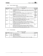
3.1.5
PCI Interface Signals
Table 3.1.5 PCI Interface Signals (1/2)
Signal Name
Type
Description
Initial State
PCICLK[5:0] Output
PCI
Clock
PCI bus clock signals.
When these clock signals are not used, the pins can be set to H using the PCICLK
Enable field of the pin configuration register (PCFG.PCICLKEN[5:0]).
All High
PCICLKIN Input
PCI
Feedback
Clock
PCI feedback clock input.
Input
PCIAD[31:0]
Input/output PCI Address and Data
Multiplexed address and data bus.
Input
C_BE[3:0]
Input/output Command and Byte Enable
Command and byte enable signals.
Input
PAR Input/output
Parity
Even parity signal for PCIAD[31:0] and C_BE[3:0]
*
.
Input
FRAME
*
Input/output
Cycle
Frame
Indicates that bus operation is in progress.
Input
IRDY
*
Input/output
Initiator
Ready
Indicates that the initiator is ready to complete data transfer.
Input
TRDY
*
Input/output
Target
Ready
Indicates that the target is ready to complete data transfer.
Input
STOP
*
Input/output
Stop
The target sends this signal to the initiator to request termination of data transfer.
Input
LOCK
*
Input
Lock
Indicates that the PCI bus master is locking (exclusively accessing) a specified memory
target on the PCI bus.
Input
ID_SEL Input
Initialization
Device
Select
Chip select signal used for configuration access.
This pin is not used in host mode. When the PCI Controller is configured in host mode,
this pin must be pulled down.
Input
Summary of Contents for TX49 TMPR4937
Page 1: ...64 Bit TX System RISC TX49 Family TMPR4937 Rev 2 0 ...
Page 4: ......
Page 13: ...Table of Contents ix TMPR4937 Revision History 1 ...
Page 14: ...Table of Contents x ...
Page 15: ...Handling Precautions ...
Page 16: ......
Page 18: ...1 Using Toshiba Semiconductors Safely 1 2 ...
Page 40: ...3 General Safety Precautions and Usage Considerations 3 18 ...
Page 42: ...4 Precautions and Usage Considerations 4 2 ...
Page 43: ...TMPR4937 2005 3 Rev 2 0 ...
Page 44: ......
Page 52: ...Chapter 1 Overview and Features 1 6 ...
Page 156: ...Chapter 7 External Bus Controller 7 56 ...
Page 491: ...Chapter 16 Removed 16 1 16 Removed ...
Page 492: ...Chapter 16 Removed 16 2 ...
Page 493: ...Chapter 17 Removed 17 1 17 Removed ...
Page 494: ...Chapter 17 Removed 17 2 ...
Page 495: ...Chapter 18 Removed 18 1 18 Removed ...
Page 496: ...Chapter 18 Removed 18 2 ...
Page 497: ...Chapter 19 Removed 19 1 19 Removed ...
Page 498: ...Chapter 19 Removed 19 2 ...
Page 506: ...Chapter 20 Extended EJTAG Interface 20 8 ...
Page 530: ...Chapter 22 Pinout and Package Information 22 10 ...
Page 542: ...Chapter 24 Parts Number when Ordering 24 2 ...


