Chapter 3 Signals
3-8
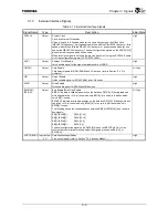
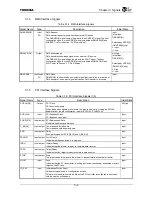
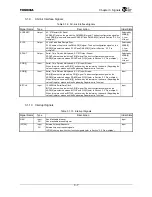
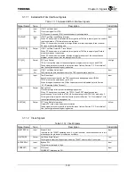
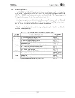
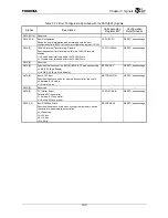
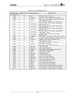
3.1.11 Extended EJTAG Interface Signals
Table 3.1.11 Extended EJTAG Interface Signals
Signal Name
Type
Description
Initial State
TCK Input
PU
JTAG Test Clock Input
Clock input signal for JTAG.
TCK is used to execute JTAG instructions and input/output data.
Input
TDI/DINT
*
Input
PU
JTAG Test Data Input/Debug Interrupt
When PC trace mode is not selected, this signal is a JTAG data input signal. It is used to
input serial data to JTAG data/instruction registers.
When PC trace mode is selected, this signal is an interrupt input signal used to cancel
PC trace mode for the debug unit.
Input
TDO/TPC[0]
Output
JTAG Test Data Output/PC Trace Output
When PC trace mode is not selected, this signal is a JTAG data output signal. Data is
output by means of serial scan.
When PC trace mode is selected, this signal outputs the value of the non-continuous
program counter in sync with the debug clock (DCLK).
High
TPC[3:1]
Output
PC Trace Output
TPC[3:1] output the value of the noncontiguous program counter in sync with DCLK.
These signals are common with the other functions (refer to Section “3.3 Pin multiplex”).
Use the configuration setting during boot-up.
All High
TMS Input
PU
JTAG Test Mode Select Input
TMS mainly controls state transition in the TAP controller state machine.
Input
TRST
*
Input
Test
Reset
Input
Asynchronous reset input for the TAP controller and debug support unit (DSU).
TRST
*
pin must be pulled down (ex.10 k
Ω
).
When this signal is deasserted, G-Bus timeout detection is disabled (refer to Section
“5.1.1 Detecting G-Bus Timeout”).
Input
DCLK Output
Debug
Clock
Clock output signal for the real-time debugging system.
When PC trace mode is selected, the TPC[3:1] and PCST signals are output
synchronously. This clock is the TX49/H3 core operating clock (CPUCLK) divided by 3.
This signal is common with the other functions (refer to Section “3.3 Pin multiplex”). Use
the configuration setting during boot-up.
Low
PCST[8:0]
Output
PC Trace Status Information
Outputs PC trace status and other information.
These signals are common with the other functions (refer to Section “3.3 Pin multiplex”).
Use the configuration setting during boot-up.
All Low
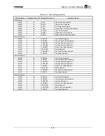
3.1.12 Clock
Signals
Table 3.1.12 Clock Signals
Signal Name
Type
Description
Initial State
MASTERCLK Input Master
Clock
Input pin for the TX4937 operating clock. A crystal resonator cannot be connected to this
pin because the pin does not contain an oscillator.
Input
HALTDOZE Output
Halt/Doze
State
Output
This signal is asserted (High output) when the TX4937 enters Halt or Doze mode.
Low
BYPASSPLL
*
Input Bypass
PLL
This pin must be fixed to High.
Input
CGRESET
*
Input
CG
Reset
CGRESET
*
initializes the CG.
Input
Summary of Contents for TX49 TMPR4937
Page 1: ...64 Bit TX System RISC TX49 Family TMPR4937 Rev 2 0 ...
Page 4: ......
Page 13: ...Table of Contents ix TMPR4937 Revision History 1 ...
Page 14: ...Table of Contents x ...
Page 15: ...Handling Precautions ...
Page 16: ......
Page 18: ...1 Using Toshiba Semiconductors Safely 1 2 ...
Page 40: ...3 General Safety Precautions and Usage Considerations 3 18 ...
Page 42: ...4 Precautions and Usage Considerations 4 2 ...
Page 43: ...TMPR4937 2005 3 Rev 2 0 ...
Page 44: ......
Page 52: ...Chapter 1 Overview and Features 1 6 ...
Page 156: ...Chapter 7 External Bus Controller 7 56 ...
Page 491: ...Chapter 16 Removed 16 1 16 Removed ...
Page 492: ...Chapter 16 Removed 16 2 ...
Page 493: ...Chapter 17 Removed 17 1 17 Removed ...
Page 494: ...Chapter 17 Removed 17 2 ...
Page 495: ...Chapter 18 Removed 18 1 18 Removed ...
Page 496: ...Chapter 18 Removed 18 2 ...
Page 497: ...Chapter 19 Removed 19 1 19 Removed ...
Page 498: ...Chapter 19 Removed 19 2 ...
Page 506: ...Chapter 20 Extended EJTAG Interface 20 8 ...
Page 530: ...Chapter 22 Pinout and Package Information 22 10 ...
Page 542: ...Chapter 24 Parts Number when Ordering 24 2 ...


