Chapter 6 Clocks
6-3
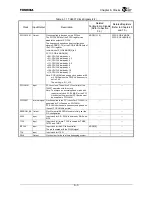
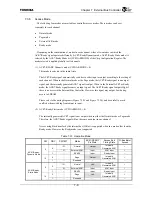
Table 6.1.1 TX4937 Clock Signals (2/2)
Clock Input/Output
Description
Related
Configuration Signals
(Refer to Section
3.2.)
Related Registers
(Refer to Chapters 5
and 10.)
PCICLK[5:0]
Output
Clock supplied to devices on the PCI bus.
The PCICLKEN bit of the PCFG register can
disable the output of PCICLK.
The frequency depends on boot configuration
signals ADDR[11:10] or the PCIDIVMODE field of
the CCFG register.
Initial Value of PCIDIVMODE[0] is 0.
CCFG_PCIDIVMODE[2:0]
=001: CPUCLK divided by 4
=011: CPUCLK divided by 4.5
=101: CPUCLK divided by 5
=111: CPUCLK divided by 5.5
=000: CPUCLK divided by 8
=010: CPUCLK divided by 9
=100: CPUCLK divided by 10
=110: CPUCLK divided by 11
Note: PCICLK[5:0] can supply clock pulses at 66
or 33 MHz when the CPUCLK frequency is
set to 300.
The setting is: 011, 010
ADDR[11:10]
CCFG.PCIDIVMODE
PCFG.PCICLKEN[5:0]
PCICLKIN Input
PCI bus clock. The built-in PCI controller of the
TX4937 operates with this clock.
Note: To achieve an accurate phase match with
the external clock, PCICLK[5:0] or the PCI
clock output from another PCI device must
be supplied to PCICLKIN.
⎯
⎯
PCICLKO Internal
signal
Clock supplied to the PCI controller. PCICLKO is
generated by PLL2 based on PCICLKIN.
PCICLKO has the same frequency and phase as
those of PCICLKIN (input pin).
⎯
⎯
EEPROM_SK Output
Clock for serial EEPROM used to initially set the
PIC configuration.
⎯
⎯
SCLK Input Input clock for SIO. SCLK is shared by SIO0 and
SIO1.
⎯
⎯
TCLK Input Input clock for timers. TCLK is shared by TMR0,
TMR1, and TMR2.
⎯
⎯
BITCLK
Input
Input clock for the AC-link controller.
The pin is shared with the PIO[2] signal.
ADDR[9]
⎯
TCK
Input
Input clock for JTAG.
⎯
⎯
DCLK
Output
Clock output for the real-time debugging system.
⎯
⎯
Summary of Contents for TX49 TMPR4937
Page 1: ...64 Bit TX System RISC TX49 Family TMPR4937 Rev 2 0 ...
Page 4: ......
Page 13: ...Table of Contents ix TMPR4937 Revision History 1 ...
Page 14: ...Table of Contents x ...
Page 15: ...Handling Precautions ...
Page 16: ......
Page 18: ...1 Using Toshiba Semiconductors Safely 1 2 ...
Page 40: ...3 General Safety Precautions and Usage Considerations 3 18 ...
Page 42: ...4 Precautions and Usage Considerations 4 2 ...
Page 43: ...TMPR4937 2005 3 Rev 2 0 ...
Page 44: ......
Page 52: ...Chapter 1 Overview and Features 1 6 ...
Page 156: ...Chapter 7 External Bus Controller 7 56 ...
Page 491: ...Chapter 16 Removed 16 1 16 Removed ...
Page 492: ...Chapter 16 Removed 16 2 ...
Page 493: ...Chapter 17 Removed 17 1 17 Removed ...
Page 494: ...Chapter 17 Removed 17 2 ...
Page 495: ...Chapter 18 Removed 18 1 18 Removed ...
Page 496: ...Chapter 18 Removed 18 2 ...
Page 497: ...Chapter 19 Removed 19 1 19 Removed ...
Page 498: ...Chapter 19 Removed 19 2 ...
Page 506: ...Chapter 20 Extended EJTAG Interface 20 8 ...
Page 530: ...Chapter 22 Pinout and Package Information 22 10 ...
Page 542: ...Chapter 24 Parts Number when Ordering 24 2 ...


