Alignment and Adjustment
Toshiba
5-3
5-2 Mechanical Adjustment
5-2-1 Tape Transport System and Adjustment Locations
The tape transport system has been adjusted precisely in the factory. Alignment is not necessary except for the
following :
1) Noise observed on the screen.
2) Tape damage.
3) Parts replacement in the tape transport system.
Lower flange height of tape guide is used as the reference for the transport adjustment.
To maintain the height of the tape guide and prevent damage, do not apply excessive force onto the main base.
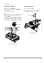
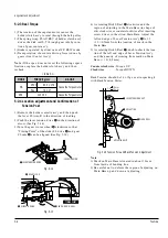
Fig. 5-3 Location of Tape Transport Adjustment
Fig. 5-4 Tape Travel Diagram
CYLINDER ASS'Y
TAKE UP REEL DISK
#8 GUIDE POST
#9 GUIDE POST
SUPPLY REEL DISK
CAPSTAN
PINCH ROLLER
GUIDE ROLLER "T"
GUIDE ROLLER "S"
FULL ERASE HEAD
#3 GUIDE POST
TENSION POST
HEIGHT SCREW
TILT SCREW
X - POSITION
ADJUST SILT
AZIMUTH SCREW
POST TENSION
MAIN BASE
FE HEAD
CYLINDER ASS'Y
PINCH ROLLER
GUIDE ROLLER "S"
GUIDE ROLLER "T"
#8 GUIDE POST
#9 GUIDE POST
CAPSTAN SHAFT
ACE HEAD
#3 GUIDE POST
Summary of Contents for W603C
Page 20: ...Reference Information Toshiba 2 13 2 2 1 IC301 LA71072M 2 2 IC Blocks ...
Page 21: ...Reference Information 2 14 Toshiba 2 2 2 IC501 AN3662 ...
Page 22: ...Reference Information Toshiba 2 15 2 2 3 IC601 MN101D02X ...
Page 23: ...Reference Information 2 16 Toshiba MEMO ...
Page 25: ...Product Specifications 3 2 Toshiba MEMO ...
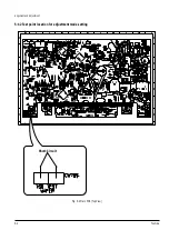
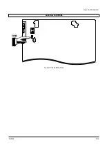
Page 56: ...Alignment and Adjustment Toshiba 5 11 Fig 5 21 Main PCB Top View VR501 Location for VR501 ...
Page 57: ...5 12 Toshiba Alignment and Adjustment MEMO ...
Page 59: ...Exploded View 6 2 Toshiba 6 1 Packing Assembly A702 A701 A702 Y101 Y102 UT01 ...
Page 63: ...Exploded View 6 6 Toshiba MEMO ...
Page 73: ...Replacement Parts List 7 10 Toshiba MEMO ...
Page 74: ...Toshiba 8 1 8 Block Diagram ...
Page 75: ...Block Diagram 8 2 Toshiba MEMO ...
Page 76: ...Toshiba 9 1 9 PCB Diagrams 9 2 9 3 9 3 9 3 9 1 Main 9 2 VFD 9 3 Jack 9 4 Key ...
Page 77: ...PCB Diagrams 9 2 Toshiba 9 1 Main ...
Page 78: ...PCB Diagrams Toshiba 9 3 9 2 VFD 9 3 Jack 9 4 Key ...
Page 79: ...PCB Diagrams 9 4 Toshiba MEMO ...
Page 82: ...Schematic Diagrams Toshiba 10 3 10 1 S M P S Power ...
Page 83: ...Schematic Diagrams 10 4 Toshiba IC601 VFD 10 2 Logic ...
Page 85: ...Schematic Diagrams 10 6 Toshiba 10 3 A V ...
Page 87: ...Schematic Diagrams 10 8 Toshiba 10 4 Hi Fi MTS ...
Page 89: ...Schematic Diagrams 10 10 Toshiba 10 5 TM Block Input Ouput ...
Page 90: ...Schematic Diagrams Toshiba 10 11 10 6 VFD ...
Page 91: ...Schematic Diagrams 10 12 Toshiba 10 7 Remote Control ...


