User's Manual l MBa8x UM 0100 l © 2021, TQ-Systems GmbH
Page 30
TQMa8x
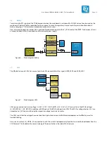
MIPI_DSI[1..0]
TQ display
adapter
Incl. PWR_EN and PWM
1,8 V; 5 V; 12V
2x USB
BLT_EN, RESET (GPIO)
I2C
USB-Hub
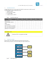
Figure 15:
Block diagram MIPI-DSI
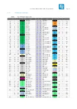
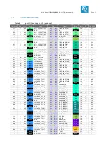
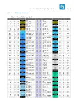
The pinout of the connector for the MIPI-DSI adapter was defined based on the existing TQ MIPI-CSI adapter. Control signals that
are not included in the corresponding bus are provided via GPIO. The differential DSI signals are extended and have a differential
impedance of 100 Ω. Furthermore, all signal lines are provided with ESD protection.
A total of up to 1.5 Gbps can be transmitted. The supported image/video formats can be found in the i.MX 8 specification.
The power drawn from the connectors must be subtracted from the power budget of the pin headers in each case!
Table 19: TQ MIPI-DSI adapter
Description
Signal
Nr. Nr. Signal
Description
1,8V
MIPI_DSI0_PWM
1
2
MIPI_DSI1_PWM
1,8V
-
GND
3
4
GND
-
GPIO (1,8V)
MIPI_DSI0_BLT_EN
5
6
MIPI_DSI1_BLT_EN
GPIO (1,8V)
1,8V
MIPI_DIS0_GPIO0_01
7
8
MIPI_DSI1_GPIO0_01 1,8V
GPIO (1,8V)
MIPI_DSI0_RESET#
9
10
MIPI_DSI1_RESET#
GPIO (1,8V)
1,8 V
V_1V8_STBY_DSI
11 12
V_12V_DSI
12 V
-
GND
13 14
GND
-
1,8 V
MIPI_DSI0_D3-
15 16
MIPI_DSI1_D3-
1,8 V
1,8 V
MIPI_
17 18
MIPI_
1,8 V
-
GND
19 20
GND
-
1,8 V
MIPI_DSI0_D2-
21 22
MIPI_DSI1_D2-
1,8 V
1,8 V
MIPI_
23 24
MIPI_
1,8 V
-
GND
25 26
GND
-
1,8 V
MIPI_DSI0_D1-
27 28
MIPI_DSI1_D1-
1,8 V
1,8 V
MIPI_
29 30
MIPI_
1,8 V
-
GND
31 32
GND
-
1,8 V
MIPI_DSI0_D0-
33 34
MIPI_DSI1_D0-
1,8 V
1,8 V
MIPI_
35 36
MIPI_
1,8 V
-
GND
37 38
GND
-
1,8 V
MIPI_DSI0_CLK-
39 40
MIPI_DSI1_CLK-
1,8 V
1,8 V
MIPI_D
41 42
MIPI_D
1,8 V
-
GND
43 44
GND
-
1,8 V
MIPI_DSI0_I2C_SDA
45 46
MIPI_DSI1_I2C_SDA
1,8 V
1,8 V
MIPI_DSI0_I2C_SCL
47 48
MIPI_DSI1_I2C_SCL
1,8 V
-
GND
49 50
GND
-
from USB2.0 Hub USB20_H3_DM
51 52
USB20_H4_DM
from USB2.0 Hub
from USB2.0 Hub USB20_H3_DP
53 54
USB20_H4_DP
from USB2.0 Hub
-
GND
55 56
GND
-
5 V
V_DSI0_VBUS
57 58
V_DSI1_VBUS
5 V
5 V
V_5V_STBY_DSI
59 60
V_5V_STBY_DSI
5 V
3.14.9
MIPI CSI
The TQMa8x has two MIPI-CSI interfaces with four lanes each. Both CSI interfaces are assigned an I2C, two GPIO signals (reset,
power enable) and a master clock output as standard. Trigger and sync signals are also provided with two M4 GPIOs each.
These interfaces are intended for connecting an adapter board for embedded camera modules. This allows easy accessibility and
flexibility in camera selection, but requires the use of an adapter board. Up to 1.5 Gbps are transmitted and a maximum image
format of 4K with 30 FPS is processed.
The differential CSI signals are elongated and have a differential impedance of 100 Ω.

