User's Manual l MBa8x UM 0100 l © 2021, TQ-Systems GmbH
Page 36
The SDHC controller in the TQMa8x supports SD cards with UHS I transfer mode according to the SD card standard 3.1. Transfer
rates of 104 Mbyte/s are thus possible.
3.14.18
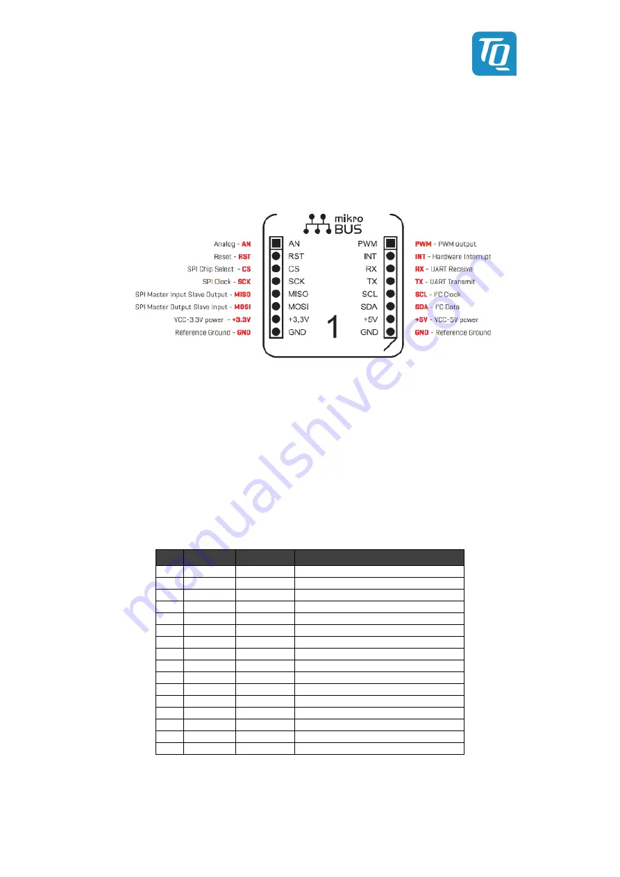
mikroBUS
A mikroBUS slot is provided for system expansion. mikroBUS is an open standard for which numerous modules or extension
boards are available. The specification explicitly stipulates that a microBUS slot must be designed with placement printing.
Figure 24:
Pinout microbus (source: MikroElektronika)
The mikroBUS modules require 3.3 V and 5 V. These are already available in the system. PTC fuses for 0.75 A are provided for fuse
protection.
With regard to the power consumption, there are no max. specified values. Since these are low-power modules, a current
consumption of 100 mA per supply voltage is provided for in the calculated current budget - this proved to be sufficient during a
random check of microBUS modules. If more power is required, this must be subtracted mathematically from the available
power at the starter kit pin headers.
Only modules with 3.3 V IO voltage can be used. Therefore, two level converters are available for the connection to the 1.8 V
logic of the TQMa8x.
Excluded from the level conversion is the analog signal (AN) with a maximum input level of 5 V, the I2C bus (I2C1_3V3) and the
reset input. The I2C bus can only be operated with 3.3 V level and must be decoupled by removing 0 ohm resistors in case of
conflict with the adapter board to be used. The reset input is decoupled via an open drain buffer.
Table 24: mikroBus signals
Pin
Identifier
Connection
Note
1-1
AN
ADC_IN0
0 Ω in series
1-2
RST
GPIO
0 Ω in series
1-3
CS
SPI0
33 Ω in series
1-4
SCK
SPI0
33 Ω in series
1-5
MISO
SPI0
100 Ω in series
1-6
MOSI
SPI0
33 Ω in series
1-7
+3.3V
-
100 mA budgeted, 0,75 A PTC
1-8
GND
GND
-
2-1
PWM
PWM2
Not available for DualMax variants
2-2
INT
GPIO
100 Ω in Serie
2-3
RX
UART2
33 Ω in Serie
2-4
TX
UART2
33 Ω in Serie
2-5
SCL
I2C1_3V3
100 Ω in series
2-6
SDA
I2C1_3V3
0 Ω in series
2-7
+5V
-
0 Ω in series
2-8
GND
GND
100 mA budgeted, 0,75 A PTC
3.14.19
ADC
For the evaluation of the ADC interface different signals and voltages are connected to the ADC inputs. The circuit is intended for
test purposes and does not allow high-precision measurements.


