background image


S

S

S

D

D

D

8

8

8

0

0

0


s

s

s

e

e

e

r

r

r

i

i

i

e

e

e

s

s

s


                                       Rev1.2 

                                      SD80 Secure Digital Card


Transcend Information Inc.


14 


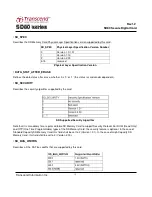
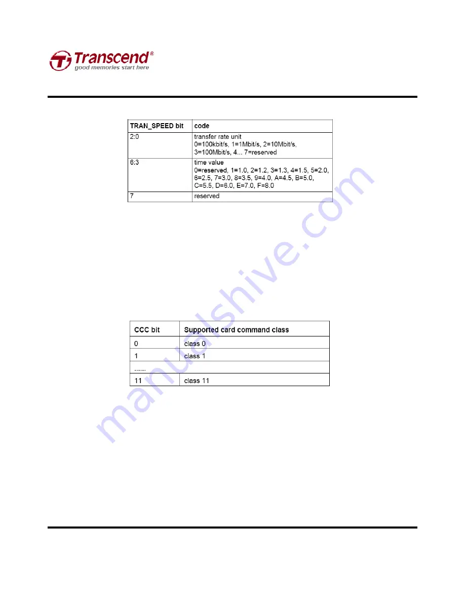
Note that for current SD Memory Cards that field must be always 0_0110_010b (032h) which is equal to 25MHz - the 
mandatory maximum operating frequency of SD Memory Card. 
 
In High-Speed mode, that field must be always 0_1011_010b (05Ah) which is equal to 50MHz. And when the timing 
mode returns to the default by CMD6 or CMD0 command, its value will be 032h. 
 

• 

CCC


The SD Memory Card command set is divided into subsets (command classes). The card command class register 
CCC defines which command classes are supported by this card. A value of ‘1’ in a CCC bit means that the 
corresponding command class is supported.  


• 

READ_BL_LEN 

 
This field is fixed to 9h, which indicates READ_BL_LEN=512 Byte. 
 

• 

READ_BL_PARTIAL 

 
This field is fixed to 0, which indicates partial block read is inhibited and only unit of block access is allowed. 
 

• 

WRITE_BLK_MISALIGN 

 
This field is fixed to 0, which indicates write access crossing physical block boundaries is always disabled in High 
Capacity SD Memory Card. 
 

• 

READ_BLK_MISALIGN


Summary of Contents for SD80 Series

Page 1: ...2 7 3 6V Operating Temperature 25 85 C Insertion removal durability 10 000 cycles Fully compatible with SD card spec v1 1 Support SD command class 0 2 4 5 7 8 Mechanical Write Protection Switch Forwa...

Page 2: ...S S SD D D8 8 80 0 0 s s se e er r ri i ie e es s s Rev1 2 SD80 Secure Digital Card Transcend Information Inc 2 Architecture...

Page 3: ...Load The total capacitance CL the CLK line of the SD Memory Card bus is the sum of the bus master capacitance CHOST the bus capacitance CBUS itself and the capacitance CCARD of each card connected to...

Page 4: ...supply voltage To meet the requirements of the JEDEC specification JESD8 1A the card input and output voltages shall be within the following specified ranges for any VDD of the allowed voltage range P...

Page 5: ...d to min VIH and max VIL Clock frequency Data Transfer Mode fPP 0 25 MHz CL 100 pF 7 cards Clock frequency Identification Mode The low freq is required for MultiMediaCard compatibility fOD 0 400 KHz C...

Page 6: ...F 7 cards Clock fall time 50 ns CL 250 pF 21 cards Inputs CMD DAT referenced to CLK Input set up time tISU 5 ns CL 25 pF 1 cards Input hold time tIH 5 ns CL 25 pF 1 cards Outputs CMD DAT referenced to...

Page 7: ...mbol Min Max Unit Remark Clock CLK All values are referred to min VIH and max VIL Clock frequency Data Transfer Mode fPP 0 50 MHz Clock low time tWL 7 ns Clock high time tWH 7 ns Clock rise time tTLH...

Page 8: ...Bending 10N Torque 0 15N m or 2 5 deg Drop test 1 5m free fall Visual inspection Shape and form No warpage no mold skin complete form no cavities surface smoothness 0 1 mm cm within contour no cracks...

Page 9: ...onditions register stores the VDD voltage profile of the card Bit 7 of OCR is newly defined for Dual Voltage Card and set to 0 in default If a Dual Voltage Card does not receive CMD8 OCR bit 7 in the...

Page 10: ...re is established to ensure uniqueness of the CID register OID A 2 character ASCII string that identifies the card OEM and or the card contents when used as a distribution media either on ROM or FLASH...

Page 11: ...erial Number is 32 bits of binary number MDT The manufacturing date composed of two hexadecimal digits one is 8 bit representing the year y and the other is four bits representing the month m The m fi...

Page 12: ...Memory Card CSD Version 2 0 is applied to only the High Capacity SD Memory Card The field name in parenthesis is set to fixed value and indicates that the host is not necessary to refer these fields T...

Page 13: ...ysical Specification Version and Card Capacity The CSD_STRUCTURE field in the CSD register indicates its structure version The following table shows the version number of the related CSD structure CSD...

Page 14: ...will be 032h CCC The SD Memory Card command set is divided into subsets command classes The card command class register CCC defines which command classes are supported by this card A value of 1 in a...

Page 15: ...pacity C_SIZE 1 512K byte As the maximum capacity of the Physical Layer Specification Version 2 00 is 32 GB the upper 6 bits of this field shall be set to 0 ERASE_BLK_EN This field is fixed to 1 which...

Page 16: ...hole card content against overwriting or erasing all write and erase commands for this card are permanently disabled The default value is 0 i e not permanently write protected TMP_WRITE_PROTECT Tempor...

Page 17: ...S S SD D D8 8 80 0 0 s s se e er r ri i ie e es s s Rev1 2 SD80 Secure Digital Card Transcend Information Inc 17...

Page 18: ...ance for extended operating conditions depending on parameters like bus length transfer rate or number of cards The CSD register carries the information about the DSR register usage The default value...

Page 19: ...ase whether it is 0 or 1 the status is card vendor dependent SD_SECURITY Describes the security algorithm supported by the card SD Supported Security Algorithm Note that it is mandatory for a regular...

Page 20: ...er r ri i ie e es s s Rev1 2 SD80 Secure Digital Card Transcend Information Inc 20 Since SD Memory Card shall support at least the two bus modes 1bit or 4bit width then any SD Card shall set at least...

Page 21: ...S S SD D D8 8 80 0 0 s s se e er r ri i ie e es s s Rev1 2 SD80 Secure Digital Card Transcend Information Inc 21 Mechanical Dimension...

Page 22: ...S S SD D D8 8 80 0 0 s s se e er r ri i ie e es s s Rev1 2 SD80 Secure Digital Card Transcend Information Inc 22...

Page 23: ...S S SD D D8 8 80 0 0 s s se e er r ri i ie e es s s Rev1 2 SD80 Secure Digital Card Transcend Information Inc 23...

Reviews: