TE0600 TRM
Revision: V3.02
Copyright © 2017 Trenz Electronic GmbH
Page
of
15
33
http://www.trenz-electronic.de
User LED
The module contains one user active-low LED connected to FPGA output pin T20. To access more LEDs,
use a carrier board and drive FPGA signals connected to B2B connectors. As LED connected to FPGA
bank with configurable VCCIO to light LED FPGA pin should in '0' (low) state. To disable LED FPGA pin
should be in 'Z' (High impedance).
Watchdog
GigaBee XS6LX has a watchdog timer that is periodically triggered by a positive or negative transition of the
WDI (watchdog input) line (FPGA pin V9). When the supervising system fails to re-trigger the watchdog
circuit within the time-out interval (min 1.1 s, typ 1.6 s, max 2.3 s), the /WDO (watchdog output) line
becomes active (low). This event also re-initializes the watchdog timer.
If zero-resistors R2 is not assembled, the watchdog is disabled (alternate assembly).
If zero-resistors R2 is assembled, the watchdog can be enabled (standard assembly). In this case there is
still two options:
To
the watchdog, after module power-up, drive the WDI signal to generate at least one transition (no
enable
matter positive or negative).
To keep watchdog
set WDI FPGA signal output to high-impedance. One way to reach this goal is
disabled,
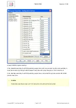
to leave FPGA pin V9 (label IO_L50N_2) undeclared in user constrains file (UCF) and set “unused IOB
pins” to “float” in the Xilinx Project Navigator options, see Fig. below.
(Project properties > Configuration options > Unused IOB Pins > Float).


