TE0600 TRM
Revision: V3.02
Copyright © 2017 Trenz Electronic GmbH
Page of
9
33
http://www.trenz-electronic.de
1.
2.
3.
4.
2.5V Power Rail
It is converted from the 3.3V rail by a linear voltage regulator and can provide up to 0.8 A to:
VCCAUX power rail;
Ethernet physical layer;
J1 connector;
J2 connector (option: if zero-resistor R80 populated and zero-resistor R79 is
populated).
is
not
VCCAUX Power
Rail
It is converted from the 3.3V rail by a linear voltage regulator and can provide up to 0.8 A to:
FPGA auxiliary circuits;
J2 connector.
VCCIO0 Power
Rail
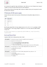
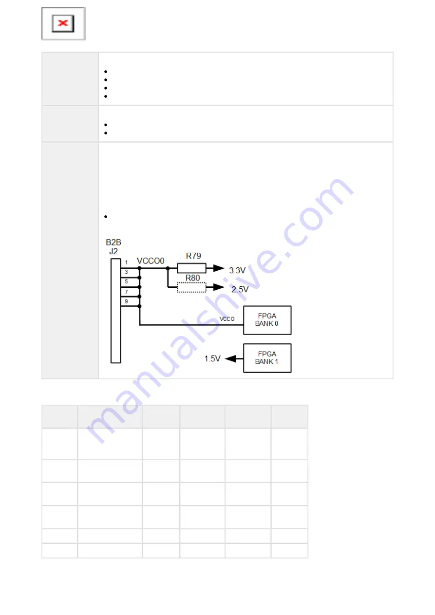
There are 4 options to supply this rail:
from 3.3 V power rail (if zero-resistor R79 populated1 and R80 is
is
not);
from 2.5 V power rail (if zero-resistor R80 populated and R79 is
is
not);
from 1.5 V power rail (if zero-resistors R79 and R80 are
populated and VCCIO0 connected to 1.5 V power
not
rail);
from an external power source through J2 B2B connector (pins 1, 3, 5, 7, 9) (if R79 and R80 are
populated)
not
It supplies:
FPGA bank 0 VCCO.
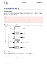
Figure below show simplified schematic of power options. Dashed resistors are not populated by default.
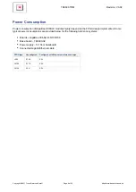
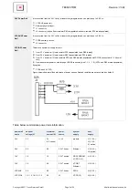
Table below summarizes power rails information.
power-rail
name
nominal
voltage(V)
maximum
current (A)
power
source
system
supply
user
supply
3.3V
3.3
2.4
(3.3 option)
J1, J2
module
J1 (1.2 A)
J2 (1.2 A,
2.1 option)
2.5V
2.5
0.8
3.3V ? linear
Ethernet
J1 (0.3 A)
J2 (option)
1.5V
1.5
1.5
3.3V ? switch
DDR3 SDRAM
VCCO (1+3)
J1 (0.3 A)
1.2V
1.2
4.0
3.3V ? switch
VCCINT
Ethernet
J1 (0.6 A)
VCCAUX
2.5
0.8
3.3V ? linear
FPGA
J2 (0.3 A)
VCCCIO0
1.2, 1.5, 1.8, 2.5, 3.3
0.9
J2
VCCO (0)
J2 (0.9 A)


