TE0600 TRM
Revision: V3.02
Copyright © 2017 Trenz Electronic GmbH
Page
of
17
33
http://www.trenz-electronic.de
Configuration Options
The FPGA on GigaBee XC6SLX board can be configured by means of the following devices:
Xilinx download cable (JTAG)
SPI Flash memory
JTAG Configuration
The FPGA can be configured through the JTAG interface. JTAG signals are connected to B2B connector
J2. When GigaBee XC6SLX board is used with the TE0603 carrier board, the JTAG interface can be
accessed via connectors J5 and J6 on the carrier board.
Flash Configuration
Default configuration option for FPGA is “Master Serial/SPI”. The bit-stream for the FPGA is stored in a
serial Flash chip (U11). See chapter 2.7 Flash Memory for additional information.
eFUSE Programming
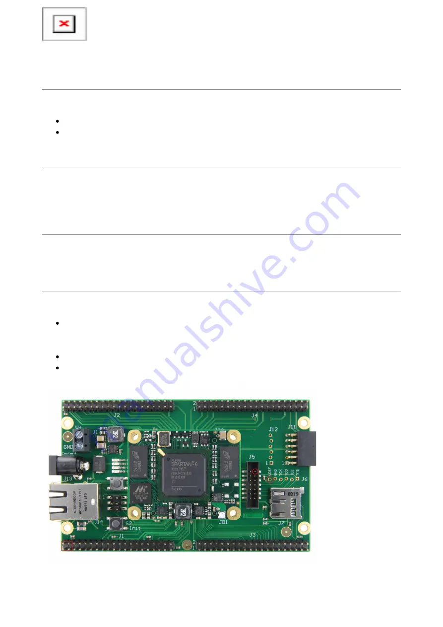
eFUSE programming feature is not directly supported by GigaBee XC6SLX modules, but it is possible to use it. To program eFUSE, please follow the steps below:
Connect VCCAUX to 3.3V power rail.
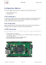
On TE0603 it can be done by connecting J5 pin 2 or J6 “VREF” (VCCAUX) to J1 any pin from 1,2,3,4
(3.3V). See Figure below.
Program eFUSE using JTAG cable and iMPACT software.
Remove power supply connections to VCCAUX


